GaN-based light-emitting diode epitaxial wafer and manufacturing method thereof
A light-emitting diode, gallium nitride-based technology, applied in semiconductor devices, electrical components, circuits, etc., can solve the problem of low light output efficiency of LED chips, and achieve the effect of increasing front light output
- Summary
- Abstract
- Description
- Claims
- Application Information
AI Technical Summary
Problems solved by technology
Method used
Image

Examples
Embodiment 1
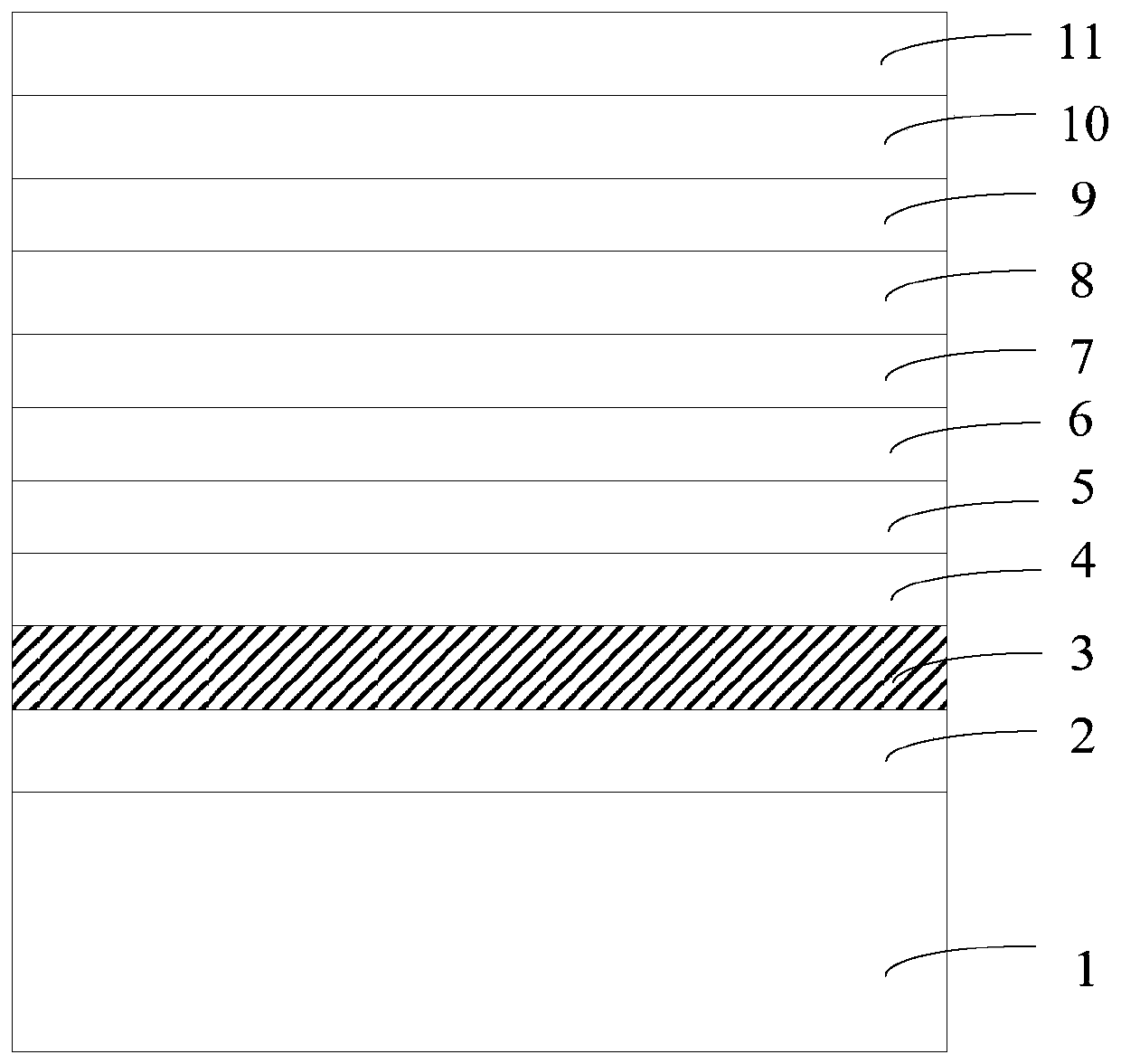
[0027] An embodiment of the present invention provides a GaN-based light-emitting diode epitaxial wafer, figure 1 It is a schematic structural diagram of a gallium nitride-based light-emitting diode epitaxial wafer provided by an embodiment of the present invention, as shown in figure 1 As shown, the gallium nitride-based light-emitting diode includes a substrate 1, and a low-temperature buffer layer 2, a reflective layer 3, a high-temperature buffer layer 4, an N-type layer 5, a shallow well layer 6, and a multi-quantum layer stacked on the substrate 1 in sequence. Well active layer 7 , low-temperature P-type layer 8 , P-type electron blocking layer 9 , high-temperature P-type layer 10 , and P-type contact layer 11 .
[0028] Wherein, reflective layer 3 is Si x In the N layer, 0<x<1, the concentration of Si in the reflective layer 3 decreases gradually from the side close to the low-temperature buffer layer 2 to the side away from the low-temperature buffer layer 2 .
[002...
Embodiment 2
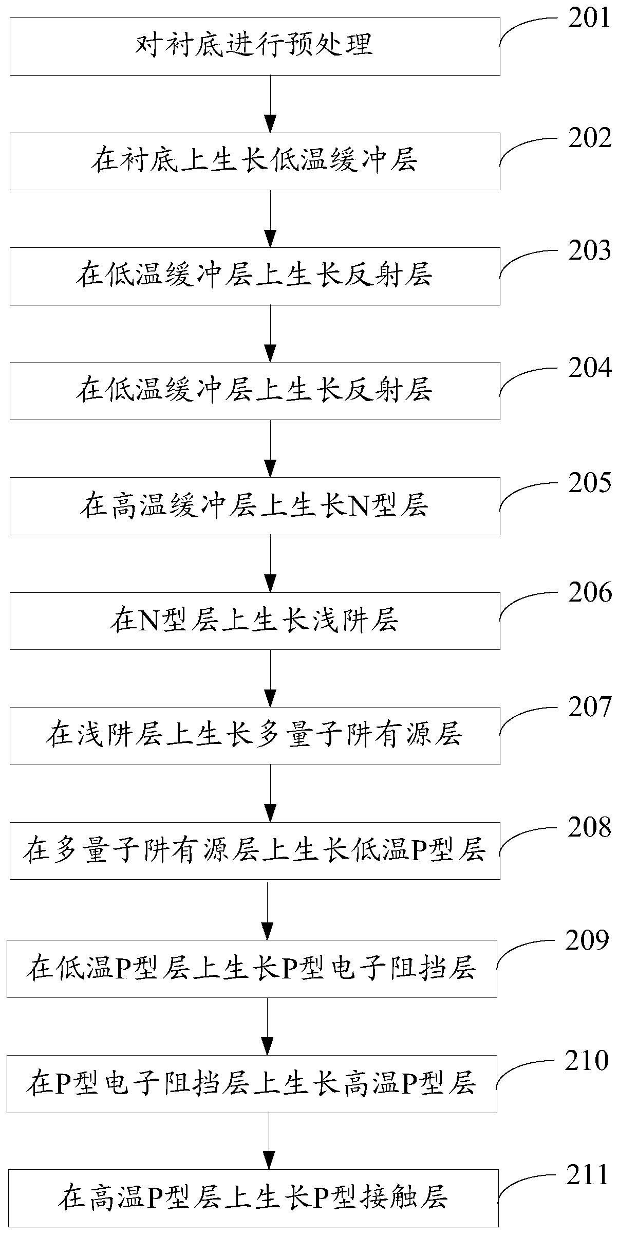
[0037] An embodiment of the present invention provides a method for manufacturing a gallium nitride-based light-emitting diode epitaxial wafer, which is suitable for the gallium nitride-based light-emitting diode epitaxial wafer provided in Embodiment 1. figure 2 It is a flow chart of a method for preparing a gallium nitride-based light-emitting diode epitaxial wafer provided by an embodiment of the present invention, as shown in figure 2 As shown, the manufacturing method includes:
[0038] Step 201, performing pretreatment on the substrate.
[0039] Optionally, the substrate is sapphire with a thickness of 630-650um.
[0040]In this embodiment, Veeco K465i or C4MOCVD (Metal Organic Chemical VaporDeposition, metal organic compound chemical vapor deposition) equipment is used to realize the LED growth method. Using high-purity H 2 (hydrogen) or high-purity N 2 (nitrogen) or high purity H 2 and high purity N 2 The mixed gas as the carrier gas, high-purity NH 3 As the N...
Embodiment 3
[0068] An embodiment of the present invention provides a method for manufacturing a gallium nitride-based light-emitting diode epitaxial wafer. In this embodiment, the reflective layer is Si x The N layer, 0.3≤x≤0.5, has a thickness of 20-40nm, and the concentration of Si in the reflective layer gradually decreases from the side close to the low-temperature buffer layer to the side away from the low-temperature buffer layer. When growing the reflective layer, the pressure in the reaction chamber is controlled at 100-500 torr, and the growth speed is 50-300 r / min during the growth process.
[0069] After finishing the growth of GaN-based light-emitting diode epitaxial wafers, lower the temperature of the reaction chamber to 600-900°C, in PN 2 The atmosphere is annealed for 10-30min, and then gradually lowered to room temperature, and then, a single 9*27mil chip is manufactured through cleaning, deposition, photolithography and etching follow-up processes.
[0070] After testin...
PUM
| Property | Measurement | Unit |
|---|---|---|
| thickness | aaaaa | aaaaa |
| pressure | aaaaa | aaaaa |
| temperature | aaaaa | aaaaa |
Abstract
Description
Claims
Application Information