Semiconductor light emitting device and manufacturing method thereof

A technology of light-emitting devices and manufacturing methods, which is applied in the direction of semiconductor devices, electrical components, circuits, etc., can solve the problems of inability to solve the problems of front light intensity and small light-emitting angle of semiconductor light-emitting devices, surface vulcanization, poor reliability, etc., and achieve simple structure, Strong anti-attenuation ability and low manufacturing cost

Pending Publication Date: 2018-05-08
SHENZHEN DADAO SEMICON CO LTD
View PDF0 Cites 0 Cited by
  • Summary
  • Abstract
  • Description
  • Claims
  • Application Information

AI Technical Summary

Problems solved by technology

Because silica gel has a certain degree of air permeability, moisture, sulfides, halides, etc. in the environment will enter the surface of the semiconductor light-emitting chip, the surface of the substrate, and the welding of the semiconductor light-emitting chip and the substrate through the silica gel-based phosphor layer, which will lead to surface vulcanization. With halogenation, serious light decay, or even failure
[0006] Therefore, due to the essential defects and deficiencies in the structure of the above-mentioned semiconductor light-emitting light source, it is impossible to solve the problems of front light intensity and small light-emitting angle of the semiconductor light-emitting device. Fast, poor reliability and other issues

Method used


Image

  • Semiconductor light emitting device and manufacturing method thereof
  • Semiconductor light emitting device and manufacturing method thereof
  • Semiconductor light emitting device and manufacturing method thereof

Examples


Embodiment Construction

[0035] In order to have a clearer understanding of the technical features, purposes and effects of the present invention, the specific implementation manners of the present invention will now be described in detail with reference to the accompanying drawings.

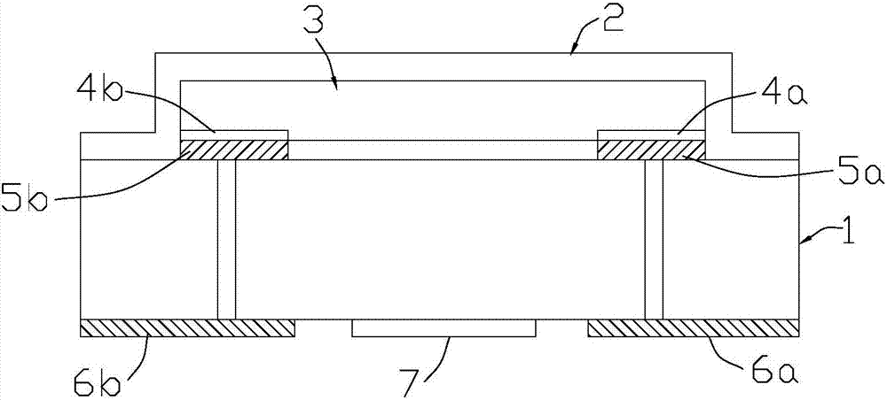
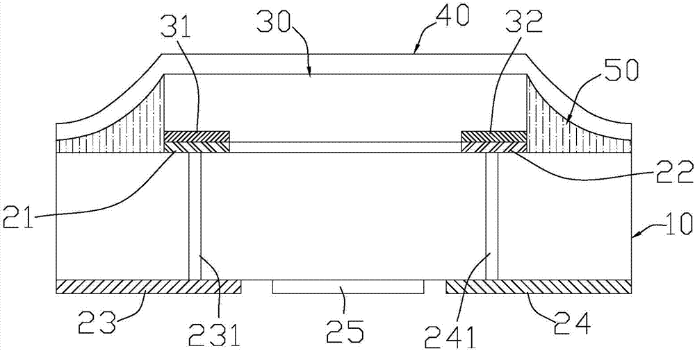
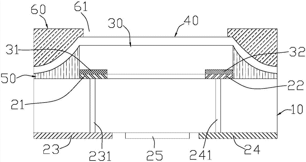
[0036] like figure 2 As shown, the semiconductor light emitting device of the first embodiment of the present invention includes a substrate 10, at least one anode pad 21 and at least one cathode pad 22 disposed on the substrate 10, and at least one semiconductor light emitting chip 30 disposed on the substrate 10. , the phosphor layer 40 that is arranged on the substrate 10 and wraps the semiconductor light-emitting chip 30, and the insulating layer 50 that is arranged on the inside of the phosphor layer 40 (towards the side of the substrate 10 and the semiconductor light-emitting chip 30); the positive electrode of the semiconductor light-emitting chip 30 31 and the negative electrode 32 are electrically connected to...


PUM


Abstract

The invention discloses a semiconductor light emitting device and a manufacturing method thereof. The semiconductor light emitting device comprises a substrate, at least one positive pad and at leastone negative pad arranged on the substrate, at least one semiconductor light emitting chip arranged on the substrate, a phosphor layer arranged on the substrate and coating the semiconductor light emitting chip and an insulation layer arranged at the inner side of the phosphor layer, wherein the positive electrode and the negative electrode of the semiconductor light emitting chip are electricallyconnected with the positive pad and the negative pad respectively; the insulation layer is located between part or all of the inner surface of the phosphor layer and part or all of the surface of thesubstrate, or, between part or all of the inner surface of the phosphor layer and part or all of the side surface of the semiconductor light emitting chip. According to the semiconductor light emitting device, through arranging the structure layer to block the side surface of the semiconductor light emitting chip, side light emitting of the semiconductor light emitting chip is prevented, front light emitting of the semiconductor light emitting chip is enhanced, and the method is suitable for manufacturing a lighting lamp with high central light intensity requirements and little light emittingangle requirements.

Description

technical field [0001] The invention relates to the technical field of semiconductor light emitting devices, in particular to a semiconductor light emitting device and a manufacturing method thereof. Background technique [0002] With the improvement of luminous efficiency and the reduction of manufacturing cost, semiconductor light sources have been widely used in the fields of backlight, display and lighting. Semiconductor light sources include LEDs, COBs, modules, light panels, light strips and many other types. In the near future, semiconductor light sources may replace traditional light sources as the main light source for general lighting. [0003] Common semiconductor light source (semiconductor light emitting device) structure such as figure 1 As shown, it includes a substrate 1, a phosphor layer 2 disposed on the substrate, a semiconductor light-emitting chip 3, a chip positive electrode 4a and a chip negative electrode 4b, a positive electrode pad 5a and a negati...

Claims


Application Information

Patent Timeline
Patent Type & Authority Applications(China)
IPC IPC(8): H01L33/48H01L33/58H01L33/62H01L33/50H01L33/00
CPCH01L33/005H01L33/48H01L33/50H01L33/58H01L33/62
Inventor 李刚
Owner SHENZHEN DADAO SEMICON CO LTD
Why Eureka
Try Eureka