A light-emitting diode epitaxial wafer and its manufacturing method

A technology of light-emitting diodes and manufacturing methods, which is applied to semiconductor devices, electrical components, circuits, etc., can solve problems such as low luminous efficiency and limited luminous area, and achieve the effects of increasing the luminous area, improving luminous brightness, and enhancing frontal light output

Active Publication Date: 2019-11-29
HC SEMITEK ZHEJIANG CO LTD
View PDF3 Cites 0 Cited by
  • Summary
  • Abstract
  • Description
  • Claims
  • Application Information

AI Technical Summary

Problems solved by technology

[0006] The embodiment of the present invention provides a light-emitting diode epitaxial wafer and its manufacturing method, which can solve the problem of low luminous efficiency due to the limited light-emitting area in the prior art

Method used


Image

  • A light-emitting diode epitaxial wafer and its manufacturing method
  • A light-emitting diode epitaxial wafer and its manufacturing method
  • A light-emitting diode epitaxial wafer and its manufacturing method

Examples


Embodiment Construction

[0038] In order to make the object, technical solution and advantages of the present invention clearer, the implementation manner of the present invention will be further described in detail below in conjunction with the accompanying drawings.

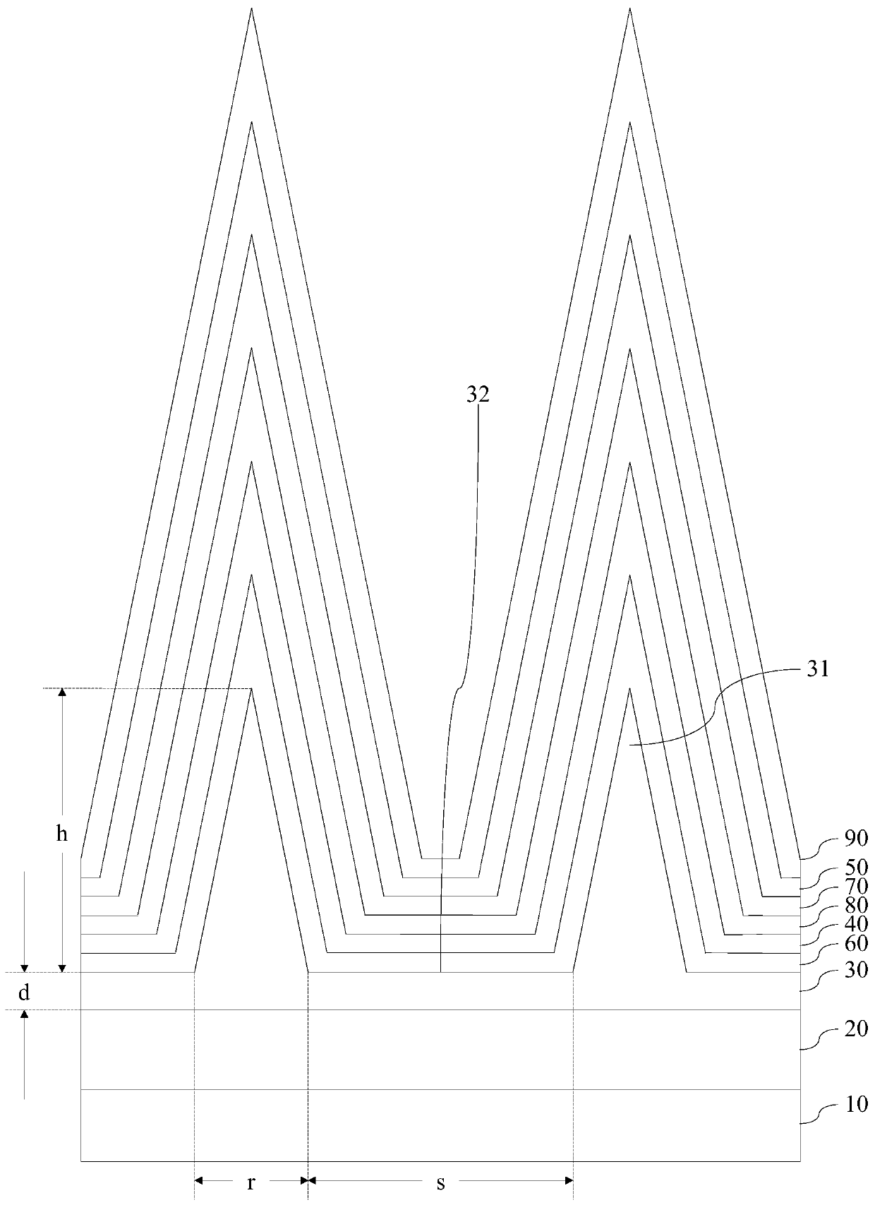
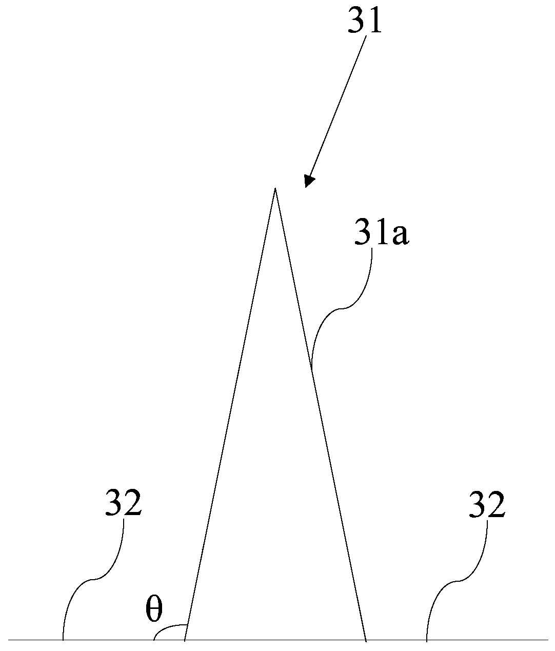
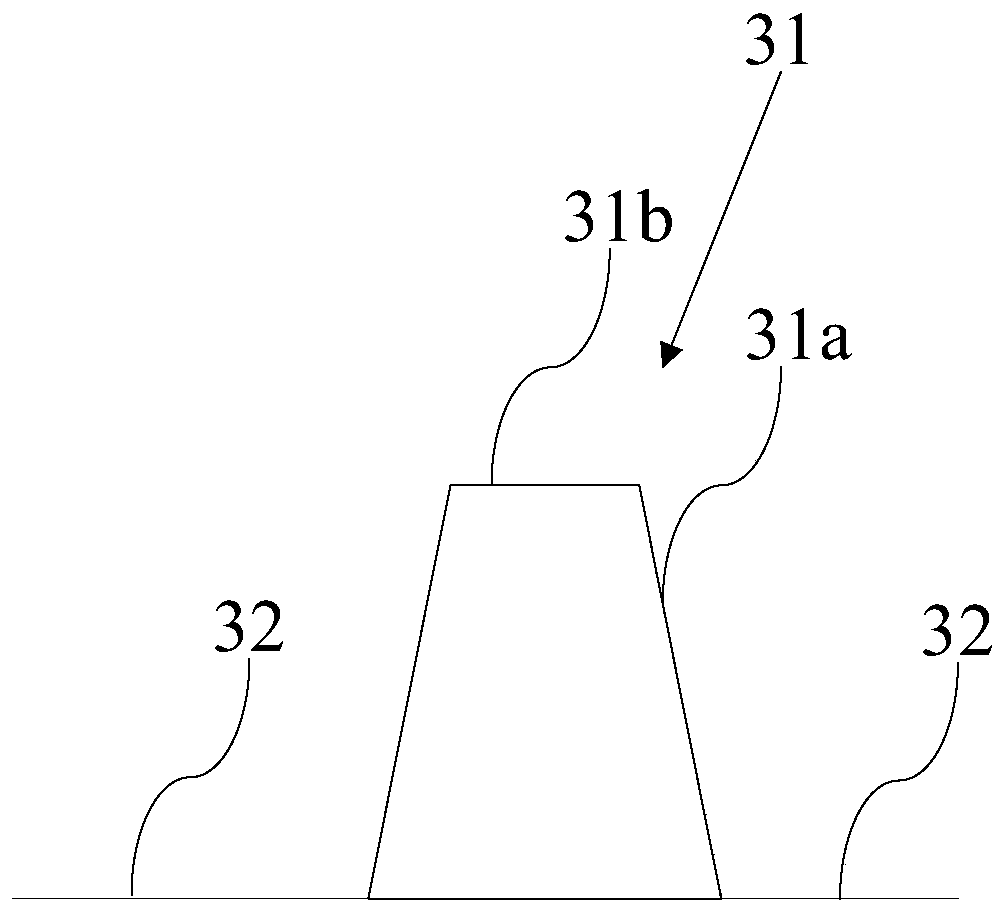
[0039] An embodiment of the present invention provides a light emitting diode epitaxial wafer, figure 1 For a structural schematic diagram of a light-emitting diode epitaxial wafer provided in an embodiment of the present invention, see figure 1 , the LED epitaxial wafer includes a substrate 10 , a buffer layer 20 , an N-type semiconductor layer 30 , an active layer 40 and a P-type semiconductor layer 50 . The buffer layer 20 is laid on the substrate 10, the first surface of the N-type semiconductor layer 30 is laid on the buffer layer 20, the second surface of the N-type semiconductor layer 30 includes a protrusion 31 and a depression 32, and the second surface is the same as The surface opposite the first surface. The active layer ...


PUM


Abstract

The invention, which belongs to the technical field of semiconductors, discloses an epitaxial wafer of a light-emitting diode and a manufacturing method thereof. The epitaxial wafer is composed of a substrate, a buffer layer, an N type semiconductor layer, an active layer, and a P type semiconductor layer. The buffer layer is laid on the substrate. A first surface of the N type semiconductor layeris laid on the buffer layer; a second surface of the N type semiconductor layer includes a convex portion and a concave portion; and the second surface is a surface opposite to the first surface. Theactive layer is laid on the convex portion and the concave portion. The P type semiconductor layer is laid on the active layer; and the sum of the thicknesses of the P type semiconductor layer and the active layer is smaller than the height of the convex portion. The surface of the convex portion includes a lateral surface intersected with the concave portion; the lateral surface is curved surface or includes a plurality of planes in end-to-end connection; and included angles between tangent planes of all points on the lateral surface or all planes in the lateral surface and the concave portion are fixed-value ones, wherein the fixed values are larger than 90 degrees and are less than 180 degrees. Therefore, the front-side light emission of the LED can be enhanced.

Description

technical field [0001] The invention relates to the technical field of semiconductors, in particular to a light-emitting diode epitaxial wafer and a manufacturing method thereof. Background technique [0002] A light-emitting diode (English: Light Emitting Diode, referred to as: LED) is a semiconductor electronic component that can emit light. LED has attracted wide attention due to its advantages of energy saving, environmental protection, high reliability, and long service life. For civil lighting, luminous efficiency and service life are the main criteria, so increasing the luminous efficiency of LEDs and improving the antistatic ability of LEDs is particularly critical for the wide application of LEDs. [0003] Epitaxial wafers are the primary products in the LED manufacturing process. The existing LED epitaxial wafer includes a substrate, a buffer layer, an N-type semiconductor layer, an active layer and a P-type semiconductor layer, and the buffer layer, the N-type s...

Claims


Application Information

Patent Timeline
Patent Type & Authority Patents(China)
IPC IPC(8): H01L33/00H01L33/12H01L33/60
CPCH01L33/005H01L33/12H01L33/60
Inventor 葛永晖郭炳磊王群吕蒙普胡加辉李鹏
Owner HC SEMITEK ZHEJIANG CO LTD
Why Eureka
Try Eureka