Large area light emitting diode light source

a light source and diode technology, applied in the direction of organic semiconductor devices, solid-state devices, thermoelectric devices, etc., to achieve the effect of large light emitting area and without risk of failur

Inactive Publication Date: 2010-06-10
OLEDWORKS GMBH
View PDF12 Cites 12 Cited by
  • Summary
  • Abstract
  • Description
  • Claims
  • Application Information

AI Technical Summary

Benefits of technology

[0005]It is an object of the present invention to provide a light emitting diode (LED) light source which can be designed to provide a large light emitting area with a homogeneous light density and without the risk of failure of larger areas due to electrical shorts.

Problems solved by technology

Further reasons of such electrical shorts are the application of a too high voltage between the electrodes or the aging of the layer structure.
The probability and number of shorts is proportional to the geometrical area of the light source, i.e. the active layer, which is in particular problematic for large area OLED or LED light sources.

Method used


Image

  • Large area light emitting diode light source
  • Large area light emitting diode light source
  • Large area light emitting diode light source

Examples


case 1

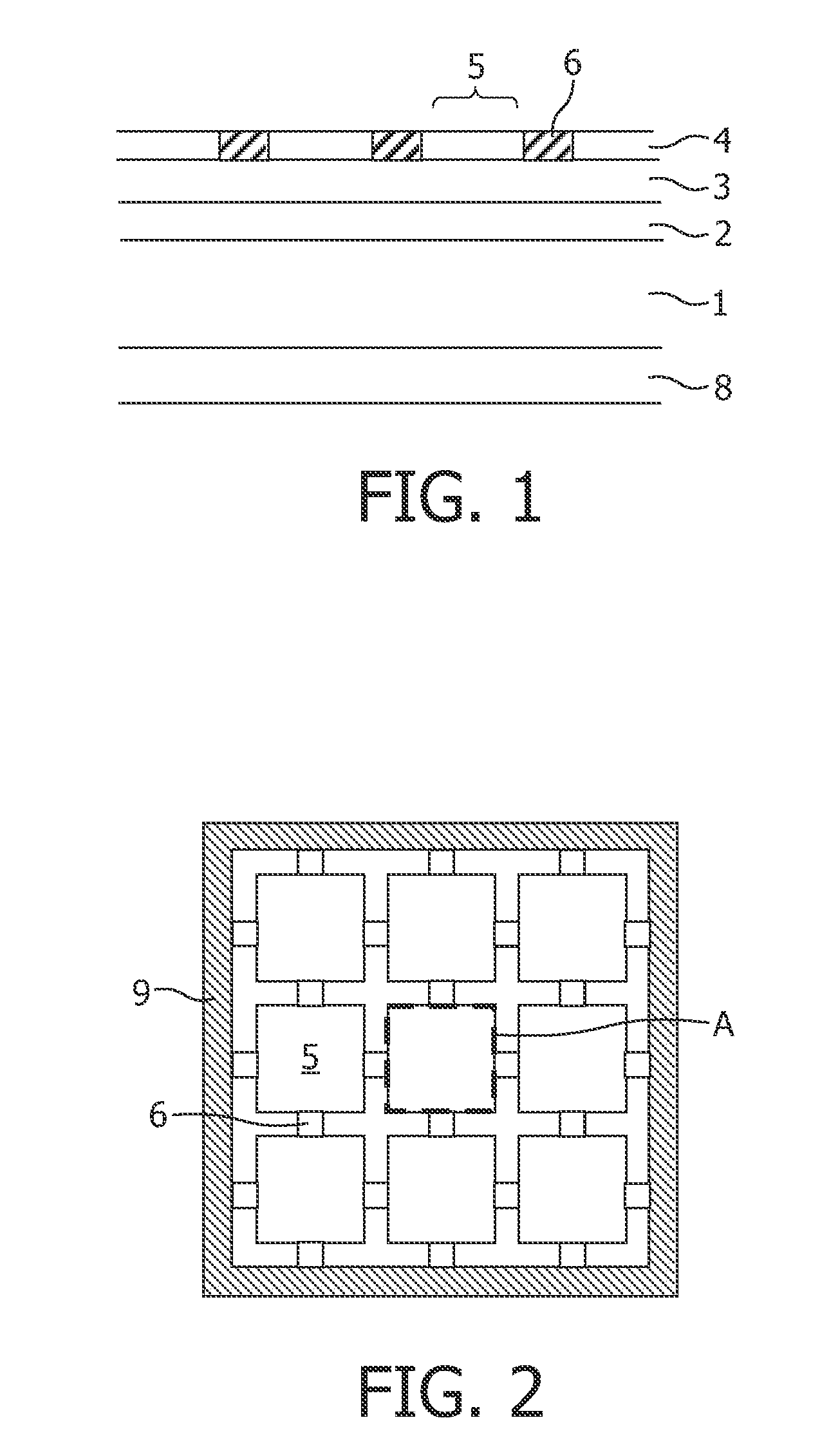
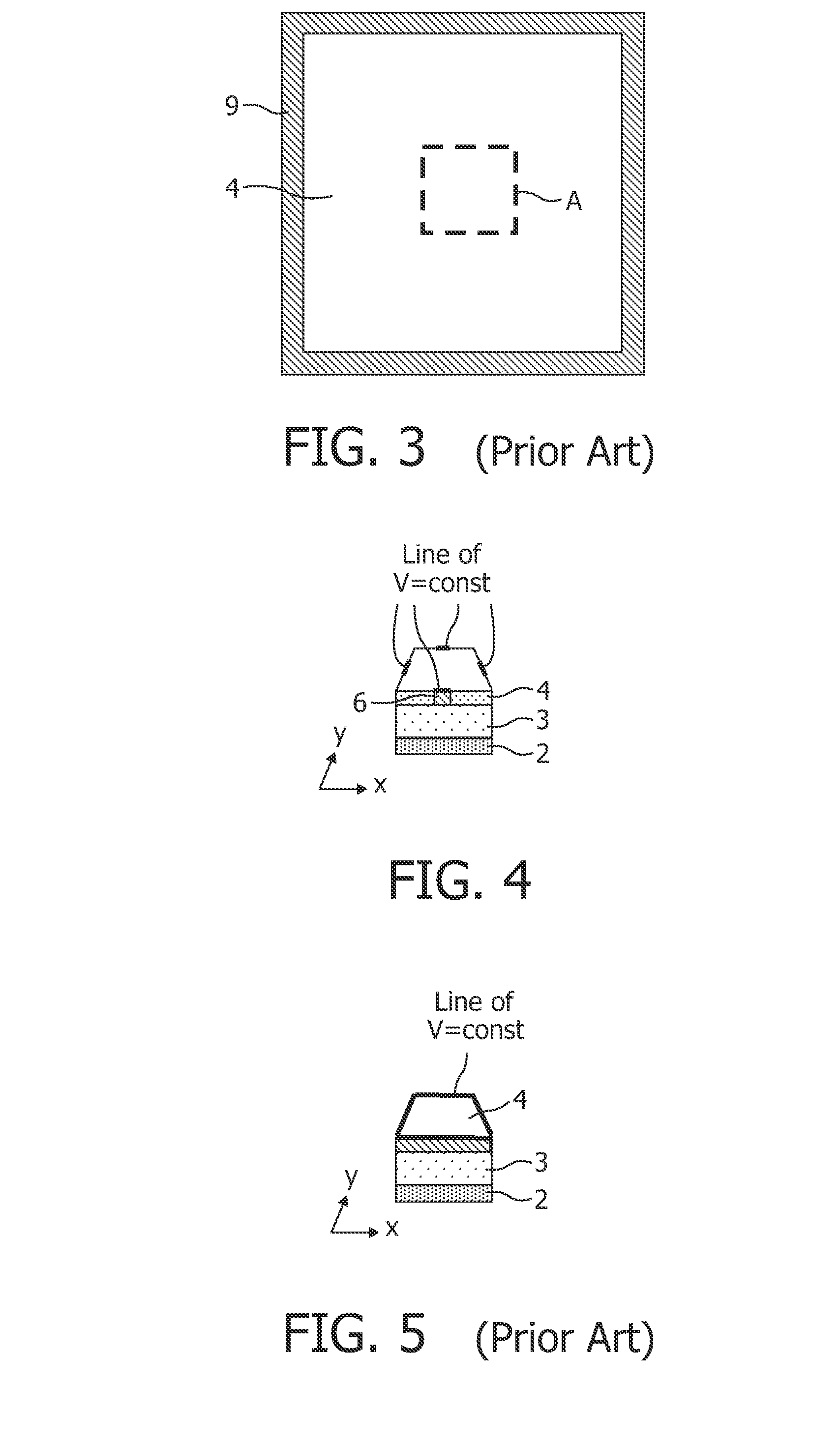
[0042] no segmented cathode (prior art)

case 2

[0043] segmented cathode with fuse elements, no short

case 3

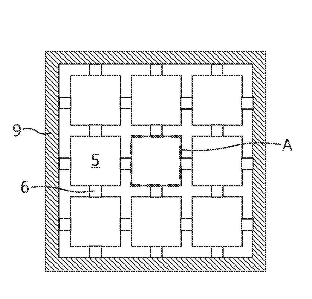
[0044] segmented cathode with fuse elements, with short in the center of the large segment

[0045]FIGS. 6 and 7 show the horizontal current density in the cathode layer, i.e. the geometric sum of the x and y components of the current density vector with and without fuses. The case of a short in the center of a segment is shown in FIG. 8 for an OLED with fuses according to the present invention. FIGS. 9 and 10 show a comparison of the brightness in cd / m2 across the OLED between an OLED of the prior art (FIG. 9) and an OLED according to the present invention (FIG. 10). For all cases the voltage along the edges is assumed to be constant and 5V. The fuse segments are square shaped of size 3 mm×3 mm and of the same thickness than the large segments.

[0046]Two observations can be made,[0047]1. introducing the fuse segments has almost no effect on the total current and light output. Even though only 7.3% of the edges are used for the current injection there is almost no increased light output...


PUM


Abstract

The present invention relates to a LED light source comprising at least one layer of light emitting material (3), in particular organic light emitting material, sandwiched between two electrode layers (2, 4). At least one of the electrode layers (2, 4) is structured to form a pattern of electrode segments (5), each electrode segment (5) being in electrical contact with at least three of its nearest neighbor electrode segments (5) via direct electrical connections (6), which are designed to act as electrical fuses between the electrode segments (5). The invention allows the design of a large area LED light source having a homogeneous light density without the risk of failure of larger light emitting areas.

Description

FIELD OF THE INVENTION[0001]The present invention relates to a light emitting diode (LED) light source comprising at least one layer of light emitting material, in particular organic light emitting material, sandwiched between two electrode layers, wherein at least one of the electrode layers is structured to form a pattern of electrode segments.BACKGROUND OF THE INVENTION[0002]Organic light emitting diodes (OLED) comprise at least one layer of an organic material which emits light in the visible spectral range upon application of an external voltage. The organic layer, also known as active layer, is sandwiched between two electrode layers in order to apply the necessary voltage for light emission. At least one of these electrode layers is of an electrically conducting material which is at least partly transparent for wavelengths of the light emitted by the active layer. It is also known to arrange one or several further layers between the electrode layers and the active layer. Thes...

Claims


Application Information

Patent Timeline
Patent Type & Authority Applications(United States)
IPC IPC(8): H01L51/52
CPCH01L27/3202H01L51/5203H01L2251/5361H01L51/5268H01L51/5221H10K59/84H10K50/805H10K50/82H10K50/854
Inventor PARAVIA, MARKHENTE, DIRK
Owner OLEDWORKS GMBH
Why Eureka
Try Eureka