Micro light-emitting diode chip

a light-emitting diode and micro-chip technology, applied in the field of light-emitting diodes, can solve the problems of reduced light-emitting area, increased process cost, and limited micro-emitting diodes, and achieves great light-emitting area ratio and easy manufacturing.

Active Publication Date: 2020-03-05
PLAYNITRIDE
View PDF0 Cites 12 Cited by
  • Summary
  • Abstract
  • Description
  • Claims
  • Application Information

AI Technical Summary

Benefits of technology

[0005]The present invention provides a micro light-emitting diode chip, which is relatively easy to manufacture and has a relatively great light emitting area ratio.
[0022]Based on the above, a length of a diagonal of the micro light-emitting diode chip in this embodiment of the present invention is greater than 0 and is less than or equal to 140 micrometers. The second electrode of the micro light-emitting diode chip is connected to the second type doped semiconductor layer on the side surface of the epitaxial structure and does not need to be connected to and contact the second type doped semiconductor layer on the top surface of the epitaxial structure by manufacturing holes with sizes of micrometers penetrating through the first type doped semiconductor layer and the light emitting layer. That is, in a process of manufacturing the micro light-emitting diode chip, precise manufacturing processes related to alignment and hole digging are reduced, so that the micro light-emitting diode chip is relatively easy to manufacture and has a relatively large light emitting area. In addition, because current carriers of the first type doped semiconductor layer and the second type doped semiconductor layer do not need to be respectively provided by setting on a same surface a position at which the first electrode and the second electrode contact, but the first electrode and the second electrode are respectively disposed on the top surface and the side surface of the epitaxial structure, the first electrode and the second electrode of which a jointing area is relatively large can be manufactured, to improve a subsequent manufacture procedure yield.

Problems solved by technology

However, the contact hole will diminish the light emitting area.
Therefore, a precise manufacturing process related to bonding alignment or hole digging is needed, and the process cost will raise.
Consequently, a micro light-emitting diode chip is limited in a manufacture procedure thereof and is not easy to manufacture.

Method used


Image

  • Micro light-emitting diode chip
  • Micro light-emitting diode chip
  • Micro light-emitting diode chip

Examples


Embodiment Construction

[0035]Reference will now be made in detail to the present preferred embodiments of the invention, examples of which are illustrated in the accompanying drawings. Wherever possible, the same reference numbers are used in the drawings and the description to refer to the same or like parts.

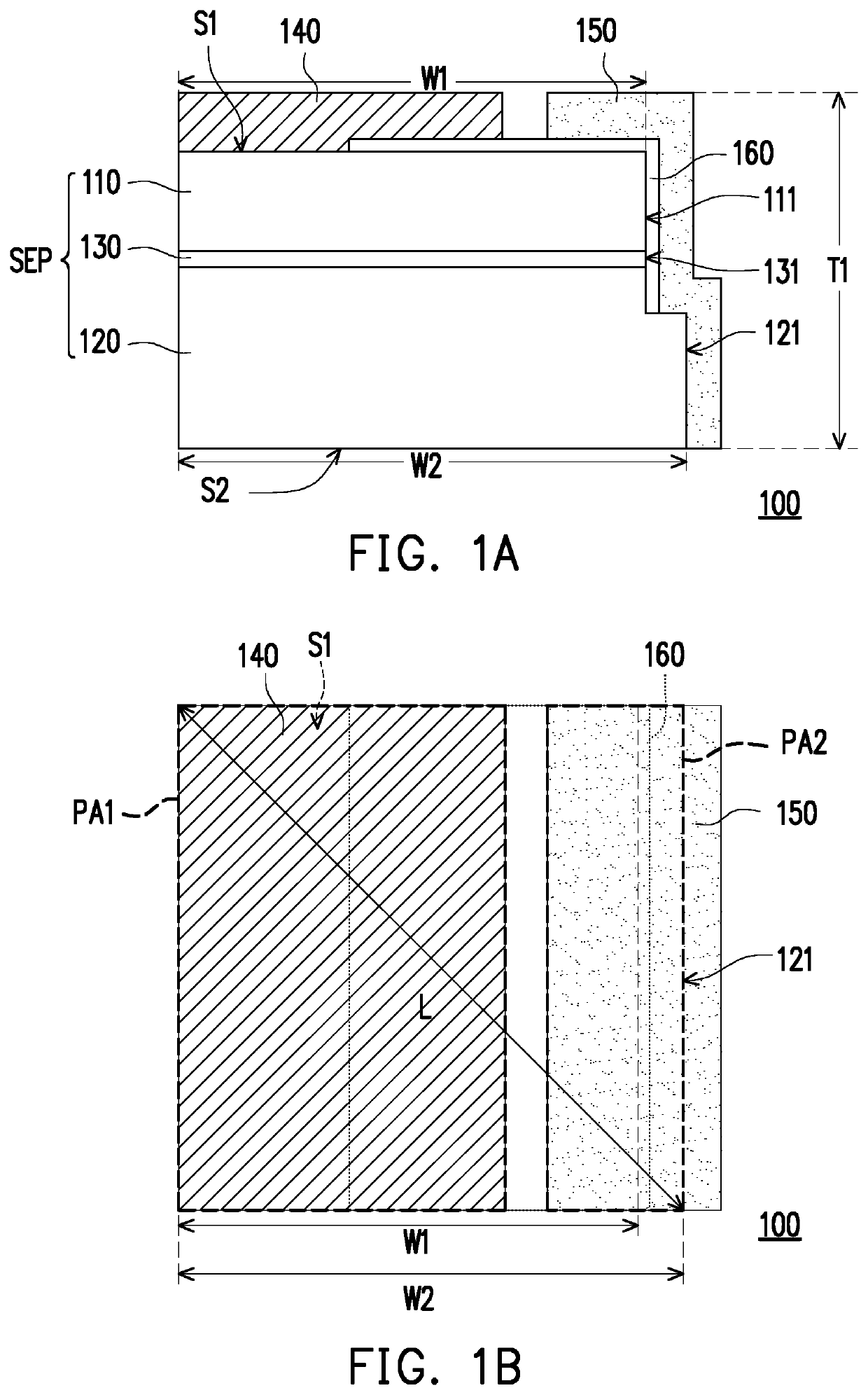
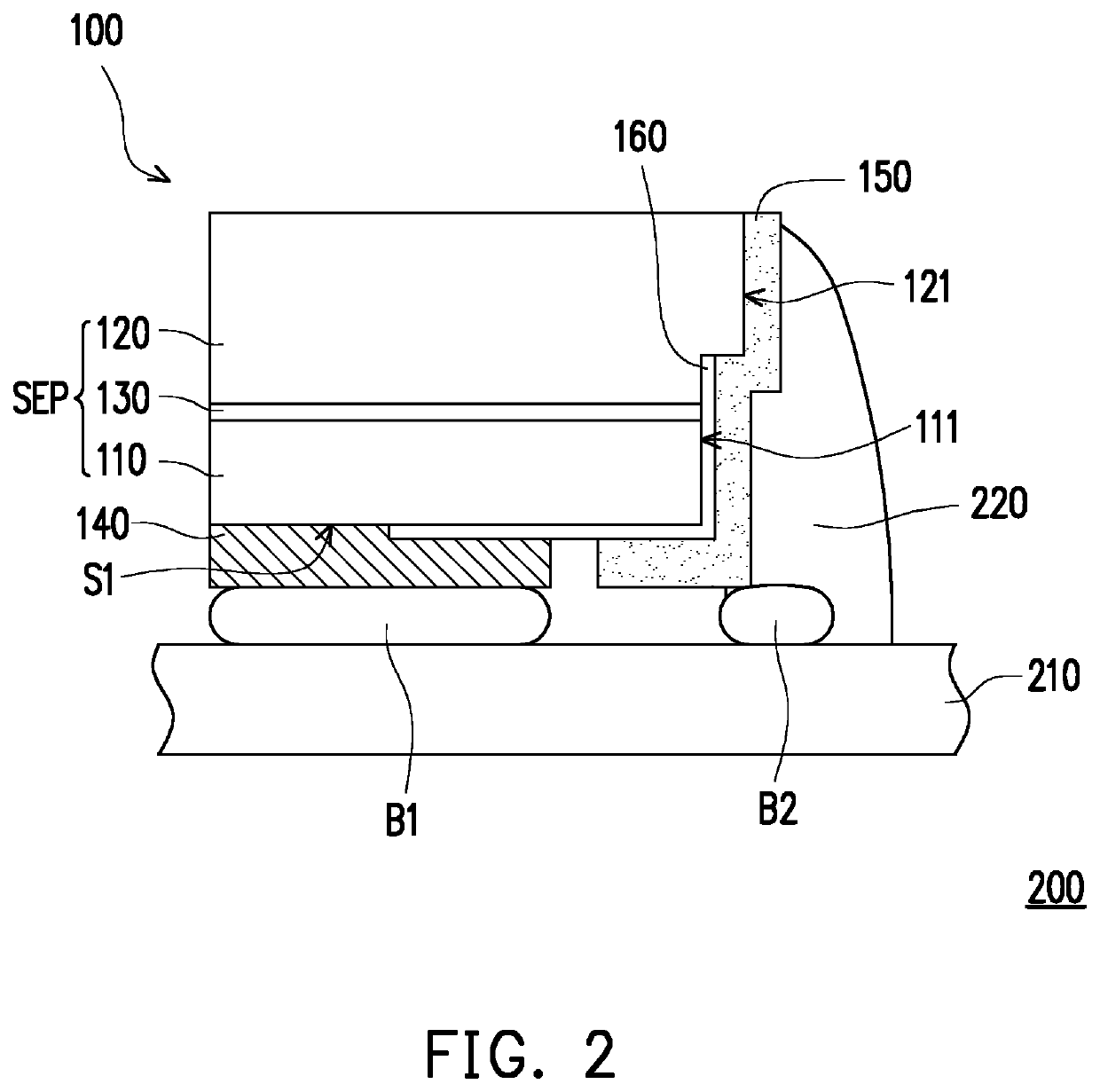
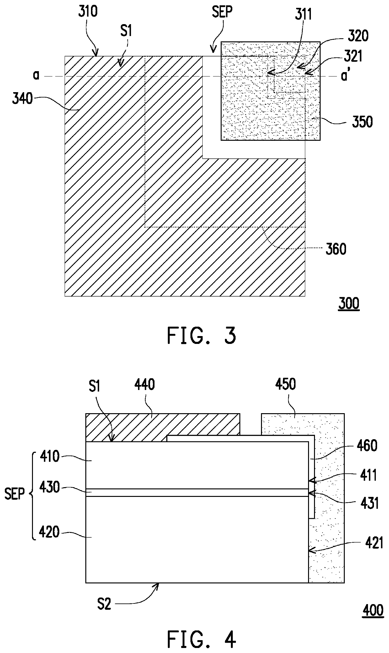
[0036]FIG. 1A is a schematic sectional view of a micro light-emitting diode chip according to an embodiment of the present invention. Referring to FIG. 1A, in this embodiment, a micro light-emitting diode (μLED) chip 100 includes an epitaxial structure SEP, an insulating layer 160, a first electrode 140, and a second electrode 150. Specifically, the epitaxial structure SEP includes a first type doped semiconductor layer 110, a second type doped semiconductor layer 120, and a light emitting layer 130 located between the first type doped semiconductor layer 110 and the second type doped semiconductor layer 120. A material of the epitaxial structure SEP may be, for example, gallium nitride (GaN), indium...


PUM

PropertyMeasurementUnit
thicknessaaaaaaaaaa
thicknessaaaaaaaaaa
thicknessaaaaaaaaaa

Abstract

A micro light-emitting diode chip includes an epitaxial structure, a first electrode, and a second electrode. The epitaxial structure includes a first type doped semiconductor layer, a light emitting layer, and a second type doped semiconductor layer, and the epitaxial structure further includes a first surface, a side surface and a second surface opposite to the first surface. The side surface of the epitaxial structure connects to an outer edge of the first surface and an outer edge of the second surface. The first electrode is disposed on the first surface, and is electrically connected to the first type doped semiconductor layer and contacts the first type doped semiconductor layer on a portion of the first surface. The second electrode is disposed on and surrounds the side surface, and electrically connected to the second type doped semiconductor layer, and directly contacts the second type doped semiconductor layer on a portion of the side surface. A length of a diagonal of the micro light-emitting diode chip is greater than 1 micrometer and is less than or equal to 140 micrometers, and a thickness of the micro light-emitting diode chip is great than 1 micrometer and is less than 10 micrometers.

Description

CROSS-REFERENCE TO RELATED APPLICATION[0001]This application is a continuation-in-part application of and claims the priority benefit of U.S. application Ser. No. 15 / 865,286, filed on Jan. 9, 2018, now allowed, which claims the priority benefit of Taiwan application serial no. 106100682, filed on Jan. 10, 2017. The entirety of each of the above-mentioned patent applications is hereby incorporated by reference herein and made a part of this specification.BACKGROUND OF THE INVENTION1. Field of the Invention[0002]The present invention relates to a light-emitting diode chip, and in particular, to a micro light-emitting diode chip.2. Description of Related Art[0003]With development of photovoltaic technologies, sizes of many photoelectric elements gradually become miniaturized. In recent years, because of breakthrough of a light-emitting diode ((Light-Emitting Diode, LED) in manufacturing sizes, currently, a micro light-emitting diode (micro-LED) display manufactured by arranging light-e...

Claims


Application Information

Patent Timeline
Patent Type & Authority Applications(United States)
IPC IPC(8): H01L33/14H01L33/22H01L33/38H01L25/075
CPCH01L33/14H01L33/22H01L33/385H01L25/0753H01L33/62
Inventor LAI, YU-HUNGLO, YU-YUNLIN, TZU-YANG
Owner PLAYNITRIDE
Why Eureka
Try Eureka