Array substrate, fabrication method thereof and display device
An array substrate and substrate technology, which is applied in the manufacture of semiconductor/solid-state devices, semiconductor devices, electrical components, etc., can solve the problems of thin-film transistor threshold voltage drift and changes in electrical characteristics, so as to improve light stability and increase luminescence area effect
- Summary
- Abstract
- Description
- Claims
- Application Information
AI Technical Summary
Problems solved by technology
Method used
Image

Examples
Embodiment 1
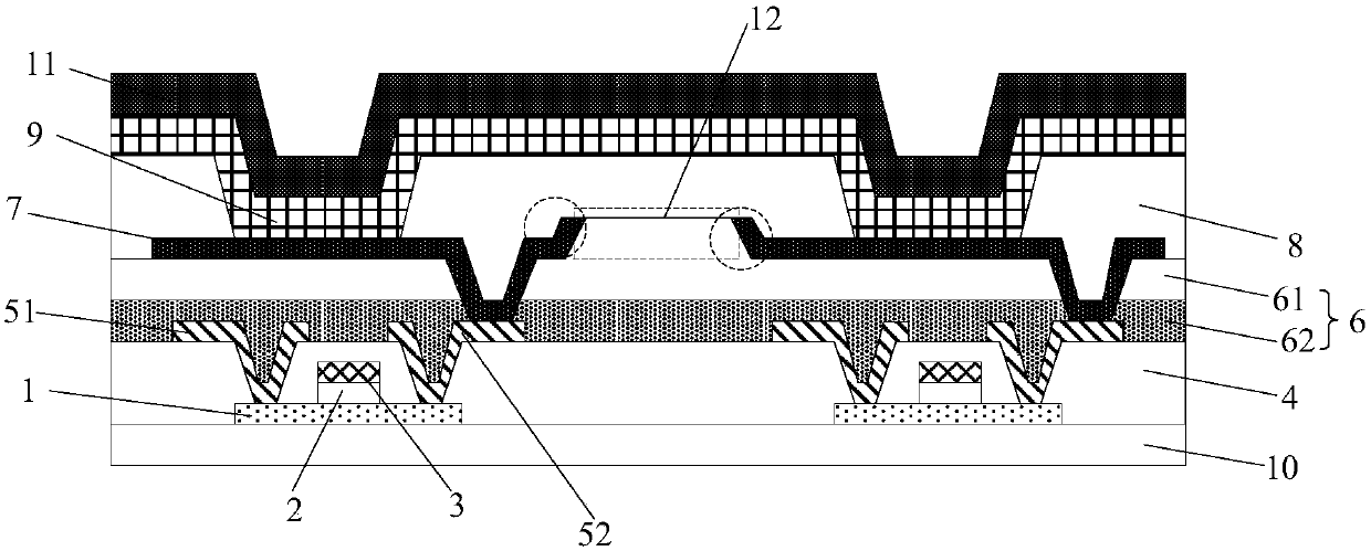
[0031] like figure 1 As shown, this embodiment provides an array substrate, including: a substrate 10, a plurality of pixel units located on the substrate 10; each of the pixel units includes an organic electroluminescence device; wherein, the organic electroluminescence The light-emitting device includes a first pole, a light-emitting layer 9, and a second pole arranged in sequence along the direction away from the substrate 10; and the material of the first pole includes a reflective material; any two adjacent organic electroluminescent devices A protruding structure 12 is arranged between the first poles of the organic electroluminescent device, and the first pole of the organic electroluminescent device extends to the side wall of the protruding structure 12, as figure 1 Shown in the dotted circle.
[0032] In the array substrate of the embodiment, since the material of the first electrode of the organic electroluminescent device is a reflective material, the organic elec...
Embodiment 2
[0041] This embodiment provides a method for preparing an array substrate, which can be used to prepare the array substrate in Embodiment 1. The preparation method includes: the step of forming a plurality of pixel units on the substrate 10; the step of forming each pixel unit includes sequentially forming the first pole, the light-emitting layer 9, and the second pole of the organic electroluminescent device on the substrate 10; and The material of the first pole includes a reflective material; and, the step of forming a raised structure 12 between the first poles of any two adjacent organic electroluminescent devices; wherein, the formed first pole of the organic electroluminescent device extending to the sidewall of the protruding structure 12 .
[0042] In the preparation method of the array substrate of the embodiment, the material of the first electrode of the formed organic electroluminescent device is a reflective material, therefore, the organic electroluminescent dev...
Embodiment 3
[0065] This embodiment provides a display device, including the array substrate in Embodiment 1.
[0066] Wherein, the display device can be a liquid crystal display device or an electroluminescent display device, such as a liquid crystal panel, an electronic paper, an OLED panel, a mobile phone, a tablet computer, a TV set, a monitor, a notebook computer, a digital photo frame, a navigator, etc. product or part.
[0067] The display device in this embodiment has better display quality.
PUM
 Abstract
Description
Claims
Application Information
 - R&D
- Intellectual Property
- Life Sciences
- Materials
- Tech Scout
- Unparalleled Data Quality
- Higher Quality Content
- 60% Fewer Hallucinations
Browse by: Latest US Patents, China's latest patents, Technical Efficacy Thesaurus, Application Domain, Technology Topic, Popular Technical Reports.
© 2025 PatSnap. All rights reserved.Legal|Privacy policy|Modern Slavery Act Transparency Statement|Sitemap|About US| Contact US: help@patsnap.com