Light emitting device

a technology of light emitting devices and crystals, which is applied in the direction of semiconductor devices, electrical devices, nanotechnology, etc., can solve the problems of degrading the light emitting characteristics of the light emitting device manufactured, experiencing defects in crystals, and difficult processes, and achieves a broad light emitting area, high light emitting efficiency, and simple structure

Inactive Publication Date: 2008-06-19
SAMSUNG ELECTRONICS CO LTD
View PDF34 Cites 13 Cited by
  • Summary
  • Abstract
  • Description
  • Claims
  • Application Information

AI Technical Summary

Benefits of technology

[0017]An aspect of the present invention provides a light emitting device of a simpler structure capable of ensuring a broad light emitting area and a high light emitting efficiency, while manufactured in a simplified and an economically efficient process.

Problems solved by technology

Here, crystals grown experience defects due to stress caused by mismatch of lattice constant and thermal expansion coefficient.
Especially, a sapphire substrate, when employed in a nitride semiconductor, results in considerable defects due to a great mismatch between a nitride and the substrate, thereby degrading light emitting characteristics of a light emitting device manufactured.
Also, in the LED of the semiconductor junction structure, the n-type semiconductor and the p-type semiconductor should be grown on one substrate, which is, however, a difficult process.

Method used


Image

  • Light emitting device
  • Light emitting device
  • Light emitting device

Examples


Embodiment Construction

[0046]Exemplary embodiments of the present invention will now be described in detail with reference to the accompanying drawings. This invention may, however, be embodied in many different forms and should not be construed as limited to the embodiments set forth therein. Rather these embodiments are provided so that this disclosure will be thorough and complete, and will fully convey the scope of the invention to those skilled in the art.

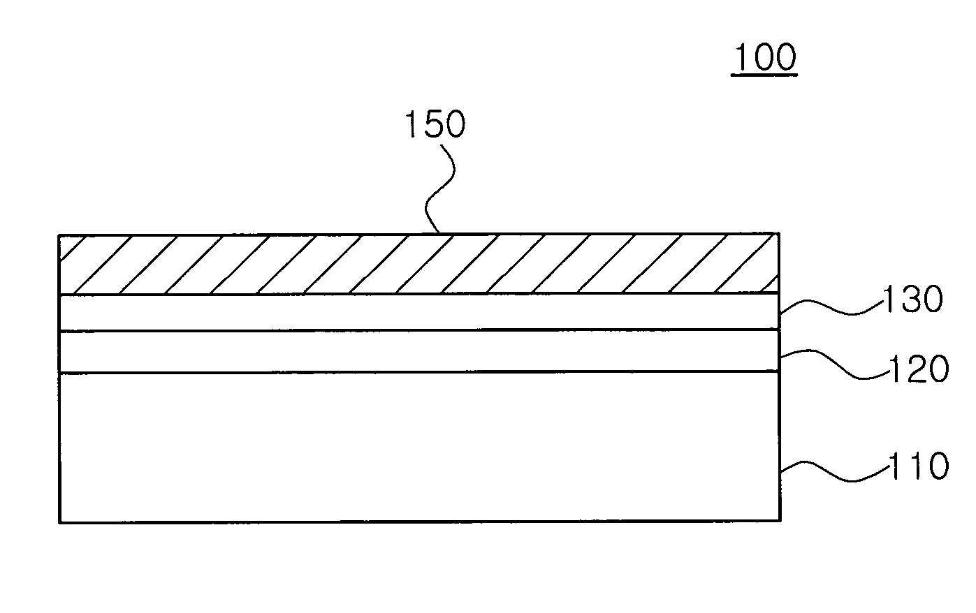
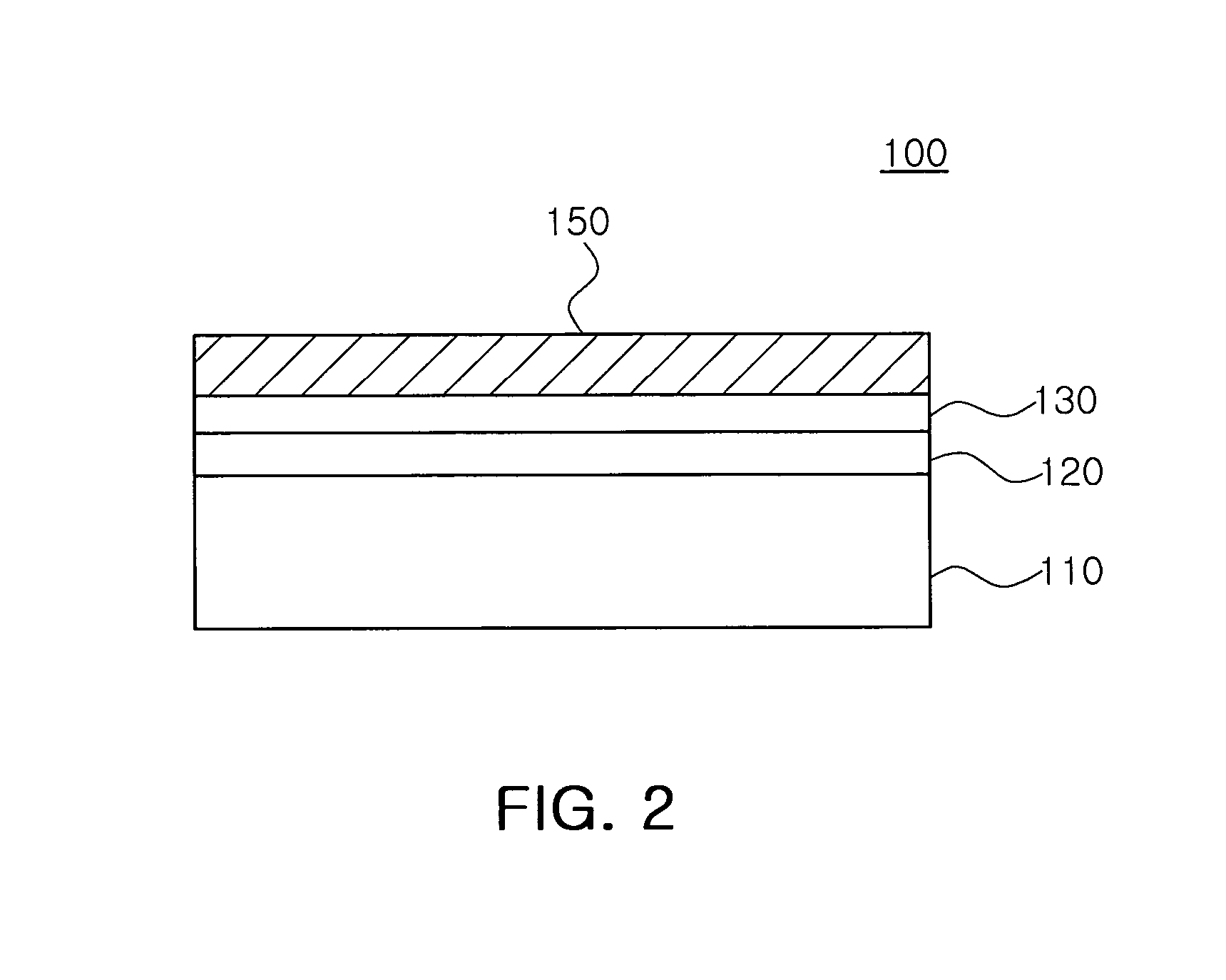
[0047]FIG. 2 is a cross-sectional view illustrating a light emitting device 100 according to an exemplary embodiment of the invention.

[0048]The light emitting device 100 of the present embodiment includes a semiconductor layer 110, an active layer 120 formed on the semiconductor layer 110 to include at least one of a quantum well structure, a quantum dot and a quantum line, an insulating layer 130 formed on the active layer 120 and a metal layer 150 formed on the insulating layer 130.

[0049]The light emitting device 100 includes the active layer 120 ...


PUM


Abstract

There is provided a light emitting device of a simpler structure, capable of ensuring a broad light emitting area and a high light emitting efficiency, while manufactured in a simplified and economically efficient process. The light emitting device including: a semiconductor layer; an active layer formed on the semiconductor layer, the active layer comprising at least one of a quantum well structure, a quantum dot and a quantum line; an insulating layer formed on the active layer; and a metal layer formed on the insulating layer.

Description

CROSS-REFERENCE TO RELATED APPLICATIONS[0001]This application claims the priorities of Korean Patent Application No. 2006-129003 filed on Dec. 15, 2006 and Korean Patent Application No. 2006-129004 filed on Dec. 15, 2006, in the Korean Intellectual Property Office, the disclosure of which is incorporated herein by reference.BACKGROUND OF THE INVENTION[0002]1. Field of the Invention[0003]The present invention relates to a light emitting device, and more particularly, a light emitting device of a simpler structure capable of ensuring a broad light emitting area and a high light emitting efficiency, while manufactured in a simplified and economically efficient process.[0004]2. Description of the Related Art[0005]In a light emitting device, a material contained therein emits light. For example, a light emitting device may have a semiconductor junction using a diode to convert energy generated by recombination of holes and electrons into light.[0006]A light emitting diode (LED) of a semi...

Claims


Application Information

Patent Timeline
Patent Type & Authority Applications(United States)
IPC IPC(8): H01L33/00H01L33/08H01L33/22
CPCH01L33/0037H01L33/08Y10S977/762H01L2933/0083H01L33/22
Inventor MOON, WON HACHOI, CHANG HWANKIM, DONG WOOHNKIM, HYUN JUN
Owner SAMSUNG ELECTRONICS CO LTD
Why Eureka
Try Eureka