Display panel, manufacturing method thereof, and display device

A display panel and display area technology, applied in nonlinear optics, instruments, optics, etc., can solve the problems of high cost, strict glass cutting accuracy and process ability, low yield, etc., and achieve the effect of good support performance

Inactive Publication Date: 2018-12-14
XIAMEN TIANMA MICRO ELECTRONICS
View PDF12 Cites 17 Cited by
  • Summary
  • Abstract
  • Description
  • Claims
  • Application Information

AI Technical Summary

Problems solved by technology

Placing the camera with an opening in the display area of ​​the display can maximize the screen-to-body ratio, but the hole-digging technology requires very strict glass cutting accuracy and process capabilities, so this method faces problems such as low production capacity, low yield, and high cost.
Moreover, it is unavoidable to squeeze and wipe the hole position during use, and the problem of liquid crystal bubbles often occurs due to insufficient support inside the hole

Method used


Image

  • Display panel, manufacturing method thereof, and display device
  • Display panel, manufacturing method thereof, and display device
  • Display panel, manufacturing method thereof, and display device

Examples


Embodiment Construction

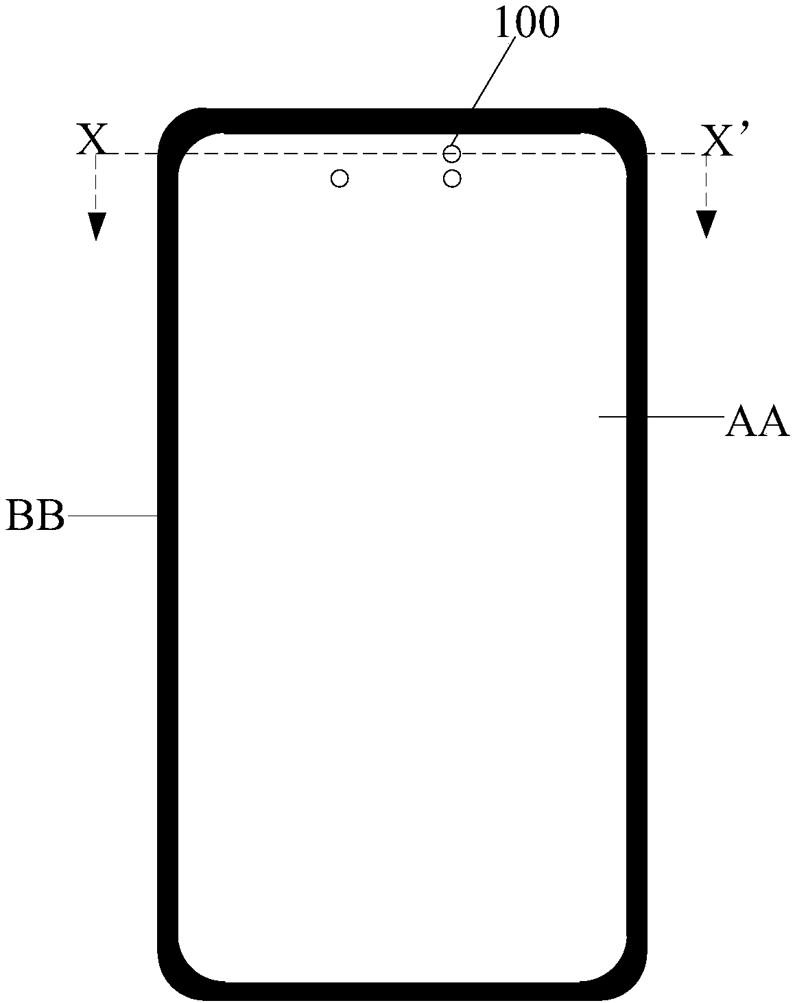
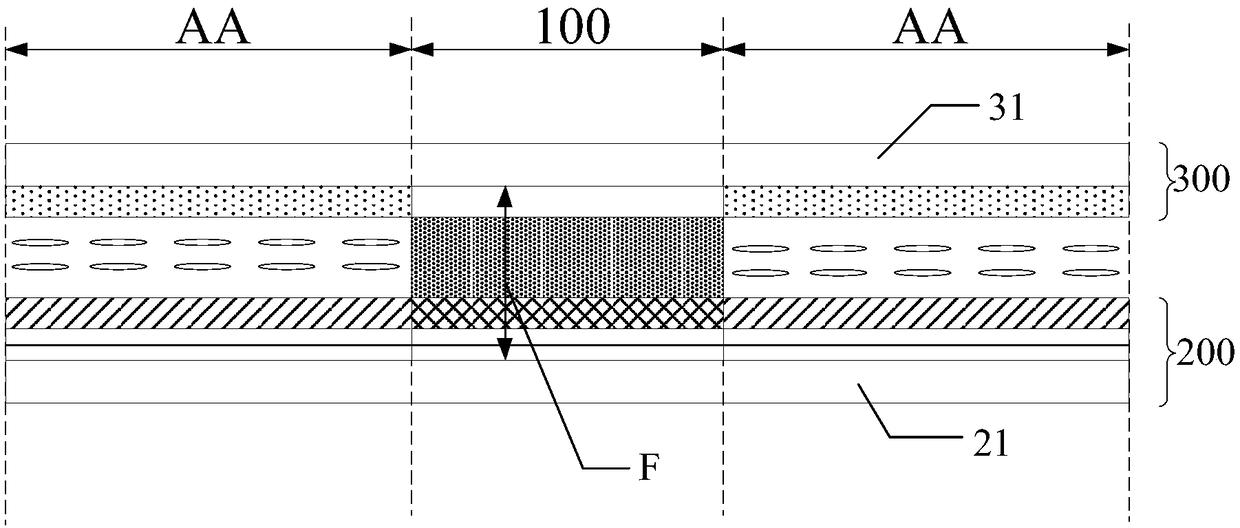
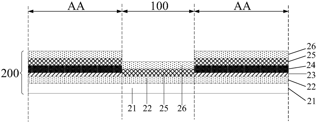
[0059] Aiming at the problems existing in the prior art, embodiments of the present invention provide a display panel, a manufacturing method thereof, and a display device for optimizing the support performance in the light-transmitting hole.

[0060] In order to make the above objects, features and advantages of the present invention more comprehensible, the present invention will be further described below in conjunction with the accompanying drawings and embodiments. Example embodiments may, however, be embodied in many forms and should not be construed as limited to the embodiments set forth herein; rather, these embodiments are provided so that this disclosure will be thorough and complete, and will fully convey the concept of example embodiments to those skilled in the art. The same reference numerals denote the same or similar structures in the drawings, and thus their repeated descriptions will be omitted. The words expressing position and direction described in the p...


PUM

PropertyMeasurementUnit
transmittivityaaaaaaaaaa

Abstract

The invention discloses a display panel, a manufacturing method thereof and a display device. The display panel comprises a display area and a non-display area surrounding the display area, wherein the display area surrounds at least one light hole; the display panel comprises a first substrate and a second substrate, which are arranged oppositely; the first substrate comprises a first transparentsubstrate; the second substrate comprises a second transparent substrate; and a compound insulation laminated structure is padded between the first transparent substrate and the second transparent substrate in the area where the light hole is located. According to the display panel disclosed by the invention, the first transparent substrate and the second transparent substrate do not need to becut to form the area where the light hole is located, the compound insulation laminated structure is just padded between the first transparent substrate and the second transparent substrate in the area where the light hole is located, the compound insulation laminated structure is made of a transmitting insulating material, so that the light transmittance of the area where the light hole is located satisfies set requirements, and meanwhile the compound insulation laminated structure also has good supporting performance.

Description

technical field [0001] The invention relates to the field of display technology, in particular to a display panel, a manufacturing method and a display device. Background technique [0002] With the continuous development of display technology, display screens such as "borderless" and "full screen" have become research hotspots in the display field. A larger screen-to-body ratio brings users a better visual experience and can display more information. Therefore, pursuing a larger screen-to-body ratio has become the mainstream development trend of display products. [0003] In the existing technology, in order to pursue a high screen-to-body ratio, the display products continue to compress the frame, and at the same time design a special-shaped screen. The full screen with a hole structure will become the latest design trend. The hole position can be used to place devices such as cameras and earpieces. Placing the camera with an opening in the display area of ​​the display c...

Claims


Application Information

Patent Timeline
Patent Type & Authority Applications(China)
IPC IPC(8): G02F1/1335G02F1/1339G02F1/1362
CPCG02F1/133512G02F1/133514G02F1/133516G02F1/13394G02F1/136209G02F1/136222
Inventor 杨雁郑斌义吴玲沈柏平
Owner XIAMEN TIANMA MICRO ELECTRONICS
Why Eureka
Try Eureka