
Pixel circuit and reading method

A pixel circuit and light-sensitive pixel technology, applied in the field of image sensors, can solve problems such as chess board fixed noise, achieve the effects of improving performance, avoiding fixed noise, and solving signal differences

Active Publication Date: 2021-01-05
思特威(上海)电子科技股份有限公司
View PDF14 Cites 0 Cited by
  • Summary
  • Abstract
  • Description
  • Claims
  • Application Information

AI Technical Summary

Problems solved by technology

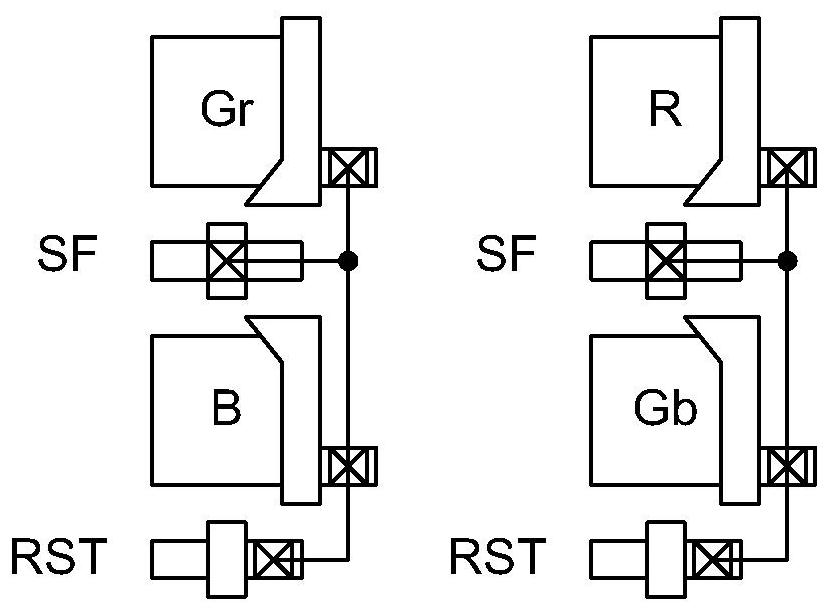
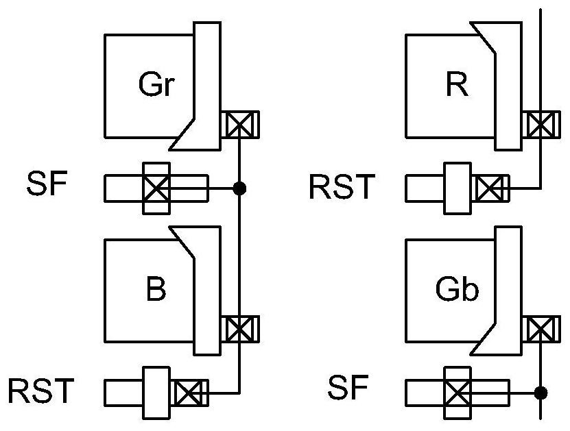
[0005] The purpose of the present invention is to provide a pixel circuit and a reading method to solve the fixed noise problem of the chess board produced by the asymmetric layout of the photosensitive pixels of the same color in the pixel circuit with a shared structure in the prior art

Method used


Image

  • Pixel circuit and reading method
  • Pixel circuit and reading method
  • Pixel circuit and reading method

Examples


Embodiment Construction

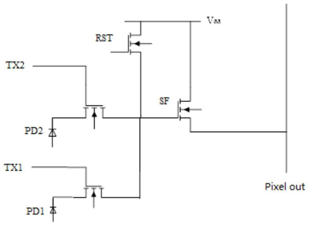
[0034] The content proposed by the present invention will be described in detail below in conjunction with each accompanying drawing. figure 2 It is a pixel circuit diagram using two photosensitive pixel sharing structures in the prior art, such as figure 2 As shown in , the photodiode PD1 and the transfer transistor TX1 constitute the first photosensitive pixel, and the photodiode PD2 and the transfer transistor TX2 constitute the second photosensitive pixel. The first light-sensing pixel and the second light-sensing pixel are shared structures, which are connected to and share the reset transistor RST and the source follower transistor SF, and the output of the pixel circuit is output from the source of the source follower transistor SF to the column line (pixel out). Multi-channel light-sensitive pixels adopt a shared structure, which can improve low-light sensitivity in smaller pixel units. The layout of the pixel circuit using the shared structure is usually designed a...


PUM


Abstract

The present invention provides a pixel circuit, which includes a pixel array composed of a plurality of pixel units arranged in rows and columns, each pixel unit includes two photosensitive pixels with a shared structure; two of each pixel unit One photosensitive pixel is arranged in two adjacent rows of the same column; two pixel units in two adjacent columns have only one photosensitive pixel arranged in the same row; the two pixel units in two adjacent columns have the same color The photosensitive pixels are respectively arranged in the two adjacent columns and arranged in the two adjacent rows, and the photosensitive pixels in the adjacent two rows are symmetrically arranged along the centerline of the row direction; each pixel unit includes a reset transistor and a source follower transistor. The invention also provides a method for reading the pixel circuit.

Description

technical field [0001] The invention relates to the technical field of image sensors, in particular to an image sensor pixel circuit and a reading method in which photosensitive pixels are arranged in a staggered manner. Background technique [0002] With the popularity of high-end smartphones, CMOS image sensors are developing towards high resolution. In order to meet a certain lens size, such as 1 / 3.2inch, 1 / 4inch, to achieve high resolution, the pixels must be designed with a smaller area. The pixel size of the commonly used 5M and 8M sensors on the market is 1.75 μm or 1.4 μm. In the process of miniaturization of pixel circuits, various technical problems will be encountered. In addition to how to improve the low-light sensitivity, another key problem is how to improve the uniformity of color and brightness of the entire pixel array. The larger the resolution and the smaller the pixels, the worse this problem becomes. In order to improve the light sensitivity, the pix...

Claims


Application Information

Patent Timeline
Patent Type & Authority Patents(China)
IPC IPC(8): H04N5/365H04N5/374H04N5/378
CPCH04N25/67H04N25/76H04N25/75
Inventor 徐辰邵泽旭陈碧
Owner 思特威(上海)电子科技股份有限公司
Learn More