
An antifuse memory unit and its data read and write circuit

A storage unit and anti-fuse technology, applied in information storage, static memory, read-only memory, etc., can solve the problems of lower reading speed and reliability, large area of ​​anti-fuse memory, large on-resistance, etc., to achieve Improve data reading speed, reduce design difficulty, and reduce the effect of on-resistance

Active Publication Date: 2021-11-05
NANJING QINHENG MICROELECTRONICS CO LTD
View PDF3 Cites 0 Cited by
  • Summary
  • Abstract
  • Description
  • Claims
  • Application Information

AI Technical Summary

Problems solved by technology

[0003] Purpose of the invention: In order to solve the problems in the prior art that the antifuse memory has a large area, high cost, large on-resistance, and reduced reading speed and reliability, the present invention proposes an antifuse memory unit and its data read-write circuit

Method used


Image

  • An antifuse memory unit and its data read and write circuit
  • An antifuse memory unit and its data read and write circuit
  • An antifuse memory unit and its data read and write circuit

Examples


Embodiment 1

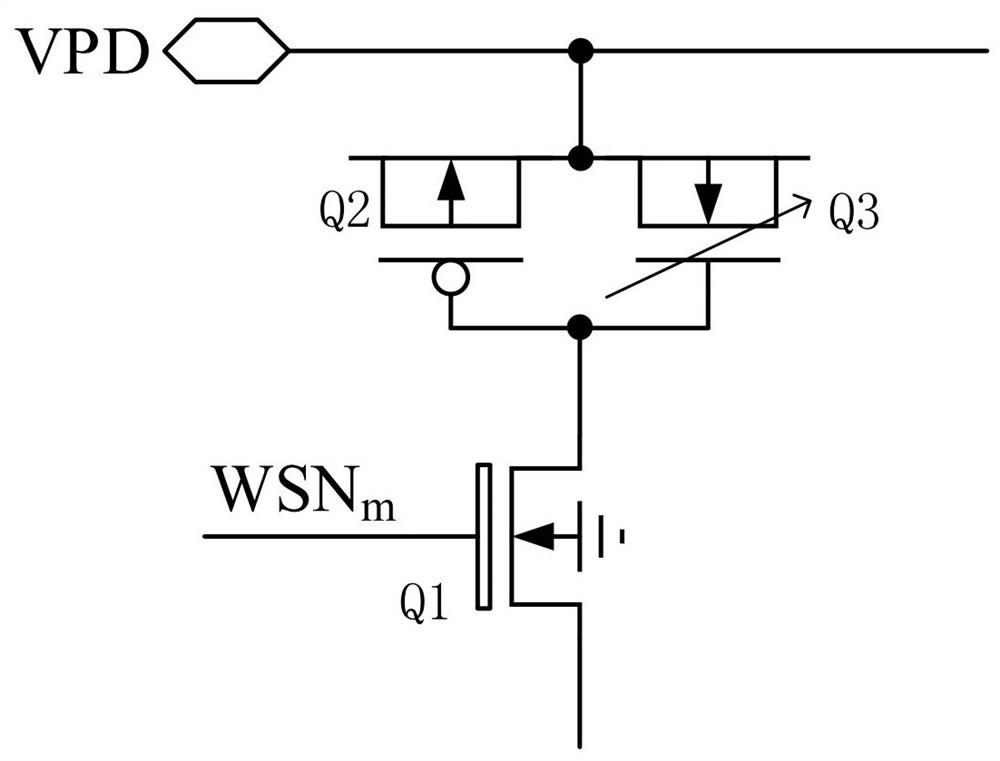
[0042] Such as figure 1 As shown, an antifuse memory unit includes a first NMOS transistor Q1, a PMOS transistor Q2 and a capacitor transistor Q3, an N well, a drain electrode of the PMOS transistor, a source electrode, a substrate, and a drain electrode, the source electrode of the capacitor transistor, The substrates are all connected to the controllable power supply VPD. The gates of the PMOS transistor and the capacitor transistor are connected to the drain of the first NMOS transistor, and the gate of the first NMOS transistor is input with a first strobe signal WSNm. The first NMOS tube Q1 adopts IO devices or 2.5V~5V high-voltage process devices, such as 2.5V / 3.3V / 5V, which can withstand the high programming voltage during occasional programming for a short time. The PMOS tube and capacitor tube use CORE core devices or 0.7V~1.8V low-voltage process devices, such as 0.9V / 1.0V / 1.2V / 1.5V / 1.8V.

[0043] From the layout point of view, as Figure 4As shown in , for ease o...

Embodiment 2

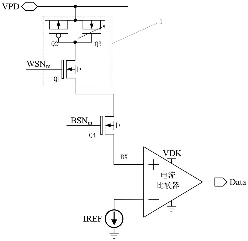
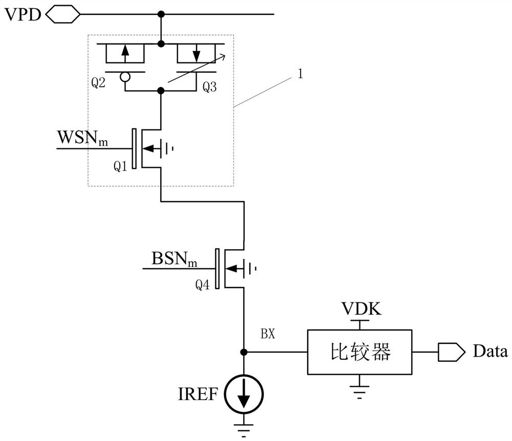
[0057] The difference between Embodiment 2 and Embodiment 1 is that in the read-write circuit of the antifuse memory unit, the source BX point of the second NMOS transistor is also connected with a pull-up transistor and a pull-down transistor. To write a valid value memory cell, except that the first strobe signal WSNm and the second strobe signal BSNm of the target cell are both set to high level, the BX point is pulled down to 0V low potential; Or write to a memory cell with an invalid value, pull up the BX point to a high potential such as 4.3V (VPD-0.7V). All the other parts are the same as the first embodiment.


PUM


Abstract

The invention discloses an anti-fuse storage unit and a data read-write circuit thereof. The anti-fuse storage unit includes a base, an N well and a non-N well area are arranged on the base, and a first NMOS transistor is arranged on the non-N well area. The gate of the first NMOS transistor is used to input the first strobe signal, and the N well is provided with a PMOS transistor and a capacitor transistor, and the gates of the PMOS transistor and the capacitor transistor are connected to the drain of the first NMOS transistor, and the PMOS transistor The drain, the source, the substrate and the drain, the source, the substrate of the capacitance tube are all connected to the controllable power supply. The invention increases the area of ​​the programmable area, reduces the on-resistance after the breakdown of the storage unit, improves the reliability, reduces the cost, and is beneficial to increase the data reading speed.

Description

technical field [0001] The invention belongs to the field of integrated circuit design, in particular to an antifuse memory unit and a data read-write circuit thereof. Background technique [0002] The development of semiconductor technology brings opportunities for product intelligence. MCU is usually indispensable for electronic intelligence, and the necessary part of MCU is memory. OTP (One-Time Programmable) memory is obtained because of its advantages of high density, less MASK levels, and low cost. widely used. At present, there are many types of OTP memories on the market, and they are constantly being updated. Early floating-gate OTPs cannot be reliably used for thinner gate oxide layers in 65nm or more advanced processes, so advanced processes generally use anti-fuse solutions. Since a memory requires tens of thousands of OTP memory cells to be implemented in an array, the structure and arrangement density of the memory cells directly determine the area of ​​the me...

Claims


Application Information

Patent Timeline
Patent Type & Authority Patents(China)
IPC IPC(8): G11C17/16G11C7/22
CPCG11C17/16G11C7/22H10B20/25H01L27/0207G11C17/18
Inventor 王春华
Owner NANJING QINHENG MICROELECTRONICS CO LTD
Learn More