Pixel defining layer and manufacturing method, display substrate and manufacturing method, display panel

A pixel-defining layer and manufacturing method technology, applied in semiconductor/solid-state device manufacturing, semiconductor devices, electrical components, etc., can solve the problems affecting the uniformity of solution film formation, avoid light leakage and cross color, and improve film formation uniformity. , the effect of reducing the degree of climbing

Active Publication Date: 2021-09-28
BOE TECH GRP CO LTD +1
View PDF9 Cites 0 Cited by
  • Summary
  • Abstract
  • Description
  • Claims
  • Application Information

AI Technical Summary

Problems solved by technology

[0005] In order to solve the problem in the prior art that the climbing of the solution for dissolving organic light-emitting materials on the side surface of the pixel defining layer affects the uniformity of film formation of the solution in the pixel area, an embodiment of the present invention provides a pixel defining layer and its manufacturing method. Method, display substrate and manufacturing method, display panel

Method used


Image

  • Pixel defining layer and manufacturing method, display substrate and manufacturing method, display panel
  • Pixel defining layer and manufacturing method, display substrate and manufacturing method, display panel
  • Pixel defining layer and manufacturing method, display substrate and manufacturing method, display panel

Examples


Embodiment Construction

[0057] In order to make the object, technical solution and advantages of the present invention clearer, the implementation manner of the present invention will be further described in detail below in conjunction with the accompanying drawings.

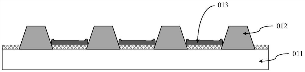
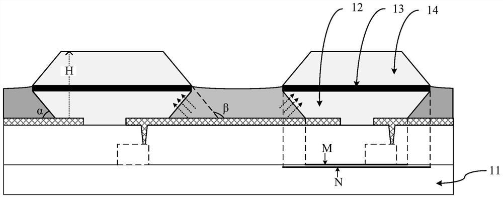
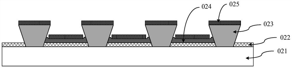
[0058] With the development of display panels towards thinner, lower power consumption and portability, a new generation of display technology represented by OLED display panels has attracted more and more attention. Compared with liquid crystal display panels, OLED display panels have the advantages of thinner and lighter, low power consumption, low driving voltage, better viewing angle, contrast ratio, and faster response speed. The film-forming methods of the organic light-emitting layer of the OLED display panel mainly include evaporation process and solution process. The evaporation process is relatively mature in small-scale applications, and this technology has been applied in mass production. The solution process mainly includ...


PUM

PropertyMeasurementUnit
thicknessaaaaaaaaaa

Abstract

The invention discloses a pixel defining layer and a manufacturing method, a display substrate and a manufacturing method, and a display panel, and belongs to the field of display technology. The pixel defining layer includes: a first sub-defining layer, a light-shielding layer and a second sub-defining layer stacked on the substrate in sequence; the orthographic projection of the surface of the first sub-defining layer close to the substrate on the substrate is located on the first sub-defining layer away from the substrate within the orthographic projection of the surface of the second sub-defining layer on the substrate, and within the orthographic projection of the light-shielding layer on the substrate; The surface is within the orthographic projection of the substrate and is located within the orthographic projection of the light shielding layer on the substrate. The invention reduces the climbing degree of the solution on the slope of the pixel defining layer and improves the uniformity of film formation. The invention is used for manufacturing OLED display panels.

Description

technical field [0001] The invention relates to the field of display technology, in particular to a pixel defining layer and a manufacturing method, a display substrate and a manufacturing method, and a display panel. Background technique [0002] An organic light-emitting diode (English: Organic Light-Emitting Diode; abbreviation: OLED) display panel includes an anode, a hole injection layer, a hole transport layer, an organic material film layer, an electron transport layer, an electron injection layer, and a cathode. Wherein, the organic material film layer can be manufactured by inkjet printing technology. When using inkjet printing technology to manufacture an organic material film layer, it is necessary to form a pixel defining layer on a glass substrate first, and then spray a solution of dissolving organic light-emitting materials onto the glass substrate on which the pixel defining layer is formed to form an organic material film layer . [0003] figure 1 It is t...

Claims


Application Information

Patent Timeline
Patent Type & Authority Patents(China)
IPC IPC(8): H01L27/32H01L51/56
CPCH10K59/122H10K71/00H10K50/865H10K59/8792H10K59/00H10K71/20H10K50/85H10K59/126H10K59/173H10K59/1201
Inventor 宫奎段献学安晖
Owner BOE TECH GRP CO LTD
Why Eureka
Try Eureka