Organic light emitting diode display panel and cutting method thereof

A technology of light-emitting diodes and display panels, which is applied in the manufacture of electrical components, electrical solid devices, and semiconductor/solid-state devices. Effect

Active Publication Date: 2019-01-11
WUHAN CHINA STAR OPTOELECTRONICS SEMICON DISPLAY TECH CO LTD
View PDF10 Cites 2 Cited by
  • Summary
  • Abstract
  • Description
  • Claims
  • Application Information

AI Technical Summary

Problems solved by technology

In the cutting method, since the OLED display panel requires multiple cutting lasers to complete the cutting process of cutting different film layers, the equipment cost is high and the manufacturing process is complicated.

Method used


Image

  • Organic light emitting diode display panel and cutting method thereof
  • Organic light emitting diode display panel and cutting method thereof
  • Organic light emitting diode display panel and cutting method thereof

Examples


Embodiment Construction

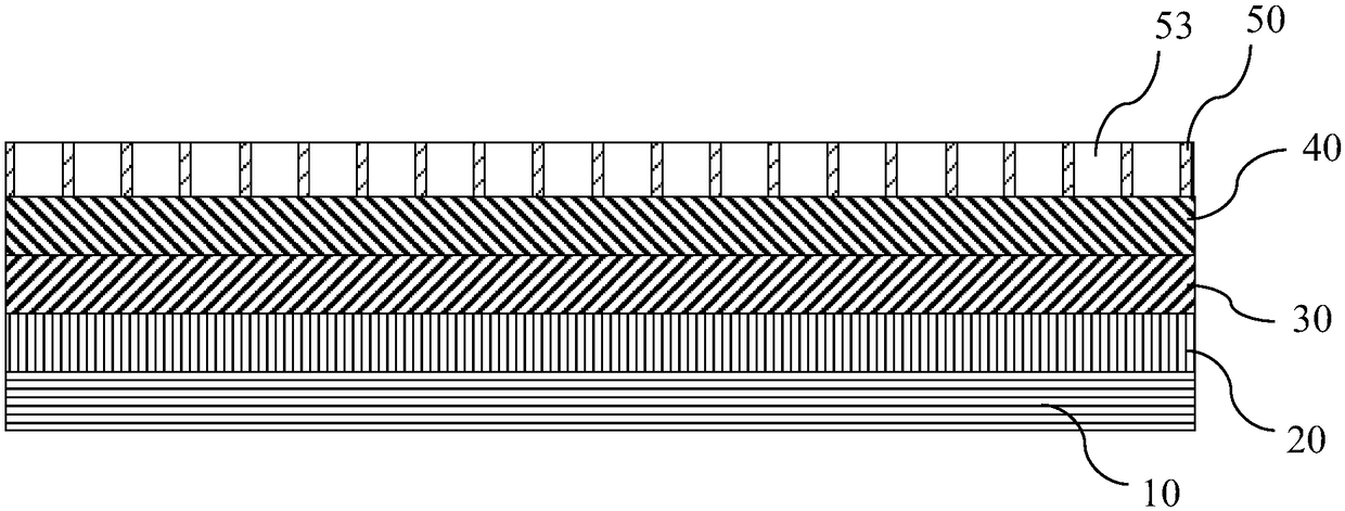
[0041] Please refer to figure 1 as well as figure 2 , the organic light-emitting diode (Organic Light-emitting Diode, OLED) display panel of the present invention comprises: a glass substrate 10, a flexible substrate 20, an organic light-emitting diode layer 30, a thin film encapsulation (Thin Film Encapsulation, TFE) layer 40, and a protective film 50 .

[0042] The flexible substrate 20 is disposed on the glass substrate 10 . Preferably, the flexible substrate 20 can be polyimide (Polyimide, PI).

[0043] The OLED layer 30 is disposed on the flexible substrate 20 .

[0044] The thin film encapsulation layer 40 is disposed on the OLED layer 30 .

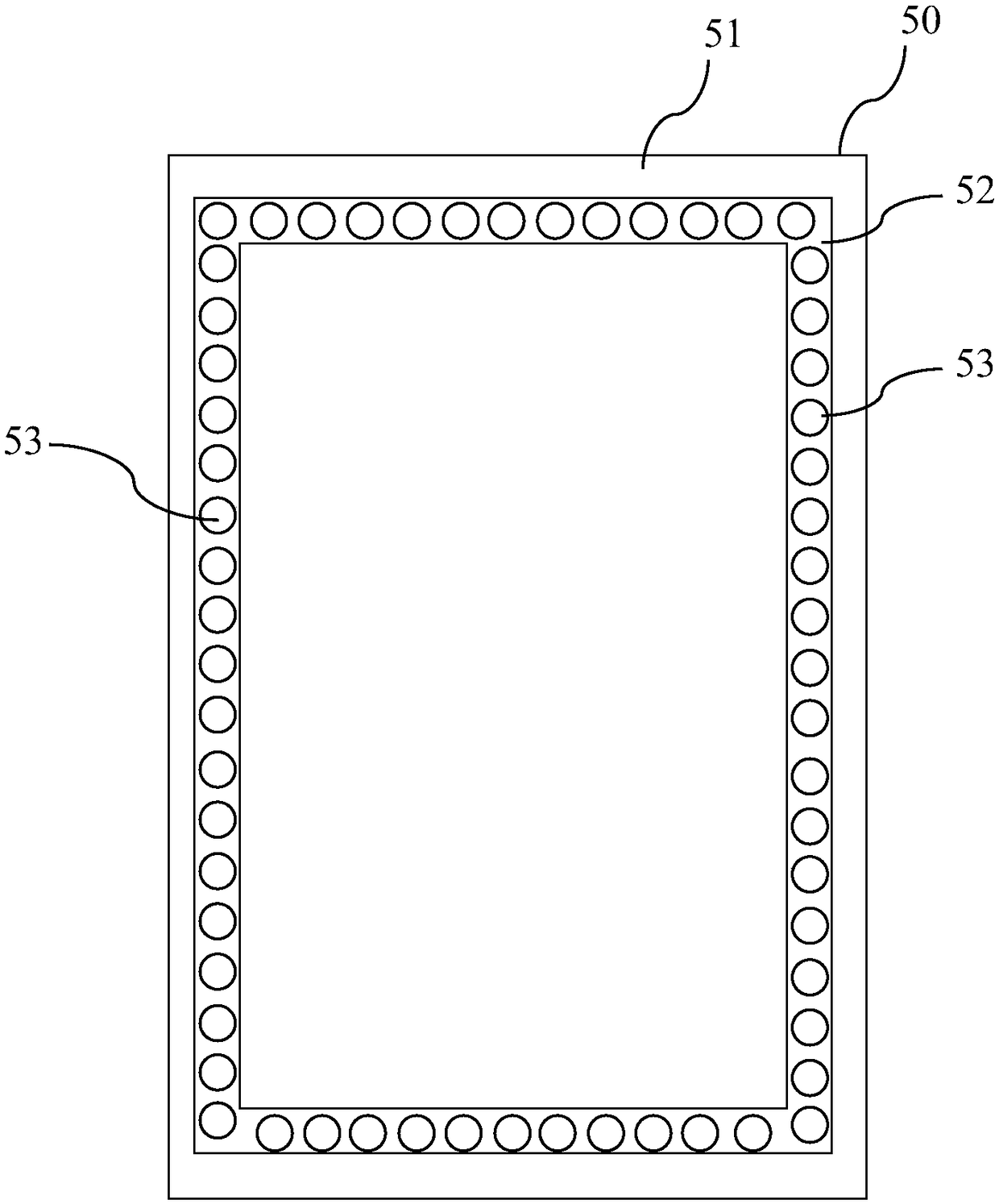
[0045] The protective film 50 is disposed on the thin film encapsulation layer 40, wherein the protective film 50 is made of polyethylene terephthalate (PET). The annular cutting road 52 is formed with a plurality of cutting perforations 53 through the cutting road 52 . Preferably, the cutting lane 52 is rectangular. Prefera...


PUM


Abstract

An organic light emitting diode display panel includes a glass substrate, a flexible substrate, an organic light emitting diode layer, a thin film encapsulation layer, and a protective film. The flexible substrate is arranged on the glass substrate. The organic light emitting diode layer is arranged on the flexible substrate. The thin film encapsulation layer is arranged on the organic light emitting diode layer. The protective film is disposed on the thin film encapsulation layer, wherein the protective film is made of polyethylene terephthalate, an annular cutting channel is formed on the protective film adjacent to the peripheral edge, and a plurality of cutting perforations are formed through the cutting channel. The protective film with cutting perforation can reduce the number of laser alternating uses for cutting the display panel, thereby simplifying the cutting process and improving the yield of the display panel.

Description

technical field [0001] The present invention relates to an organic light-emitting diode (Organic Light-emitting Diode, OLED) display panel, in particular to an organic light-emitting diode display panel and a cutting method thereof, which can reduce the number of lasers used to cut the display panel alternately. The number of times of use and the laser cutting process are simplified, thereby reducing the cost and complexity of the cutting process, thereby increasing the yield of the organic light emitting diode display panel. Background technique [0002] Organic Light-emitting Diode (OLED) display technology has the advantages of self-illumination, wide viewing angle, fast response, high brightness, low voltage, low power consumption, etc., so it is the mainstream technology adopted by the display panel manufacturing industry in the near future. [0003] In the process of cutting a large OLED display panel mother board into multiple small panels, the laser cutting process i...

Claims


Application Information

Patent Timeline
Patent Type & Authority Applications(China)
IPC IPC(8): H01L51/52H01L51/56
CPCH10K50/844H10K71/00
Inventor 袁朝煜
Owner WUHAN CHINA STAR OPTOELECTRONICS SEMICON DISPLAY TECH CO LTD
Why Eureka
Try Eureka