Organic light emitting diode display panel and cutting method thereof
A technology for light-emitting diodes and display panels, which is applied in semiconductor devices, electrical components, circuits, etc., can solve the problems of high equipment cost and complicated manufacturing process, and achieve the effect of improving cutting quality, simplifying cutting process, and reducing replacement usage.
- Summary
- Abstract
- Description
- Claims
- Application Information
AI Technical Summary
Problems solved by technology
Method used
Image
Examples
Embodiment Construction
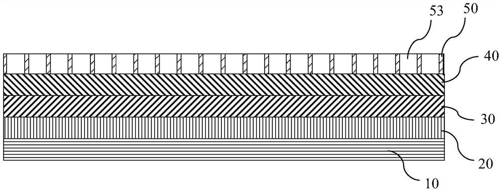
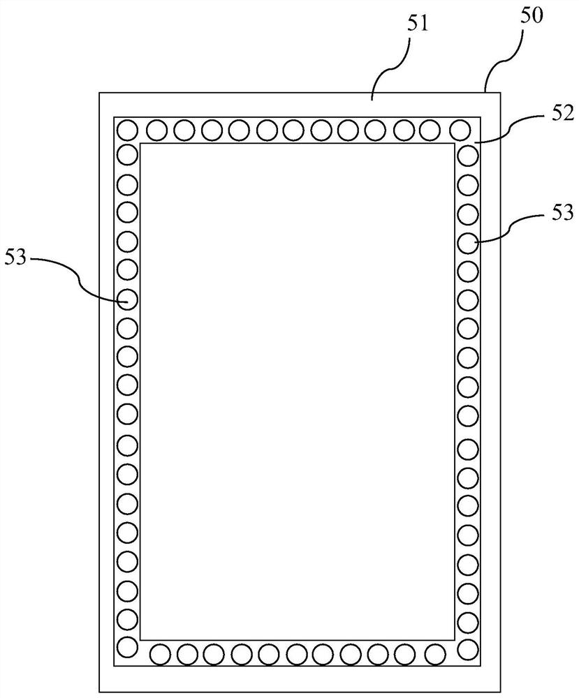
[0041] Please refer to figure 1 as well as figure 2 , the organic light-emitting diode (Organic Light-emitting Diode, OLED) display panel of the present invention comprises: a glass substrate 10, a flexible substrate 20, an organic light-emitting diode layer 30, a thin film encapsulation (Thin Film Encapsulation, TFE) layer 40, and a protective film 50 .
[0042] The flexible substrate 20 is disposed on the glass substrate 10 . Preferably, the flexible substrate 20 can be polyimide (Polyimide, PI).
[0043] The OLED layer 30 is disposed on the flexible substrate 20 .
[0044] The thin film encapsulation layer 40 is disposed on the OLED layer 30 .
[0045] The protective film 50 is disposed on the thin film encapsulation layer 40, wherein the protective film 50 is made of polyethylene terephthalate (PET). The annular cutting road 52 is formed with a plurality of cutting perforations 53 through the cutting road 52 . Preferably, the cutting lane 52 is rectangular. Prefera...
PUM
 Abstract
Description
Claims
Application Information


