Power-on mechanism

A technology of conductive sheets and electric probes, which is applied in the direction of measuring electricity, measuring electrical variables, and electronic circuit testing, etc. It can solve the problem of indentation left by LD chips, strong contact between power-on probes and LD chips, and difficulty in sensing power-on. Whether the probe has touched the LD chip, etc.

Inactive Publication Date: 2019-02-26
HISENSE BROADBAND MULTIMEDIA TECH
View PDF10 Cites 4 Cited by
  • Summary
  • Abstract
  • Description
  • Claims
  • Application Information

AI Technical Summary

Problems solved by technology

[0003] When the power-on mechanism provided in the related art is in use, it is difficult to sense whether the power-on probe has touched the LD chip, resulting in excessive contact force between the power-on probe and t

Method used


Image

  • Power-on mechanism
  • Power-on mechanism

Examples


Embodiment Construction

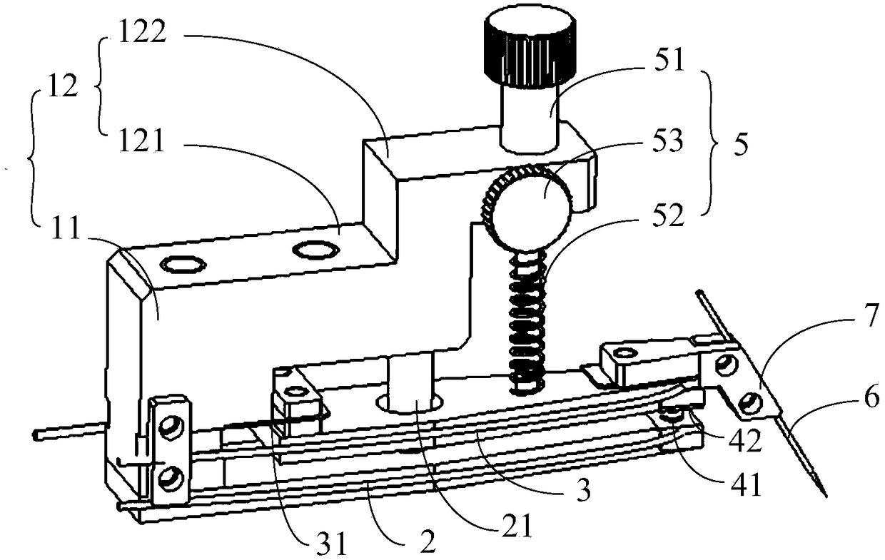
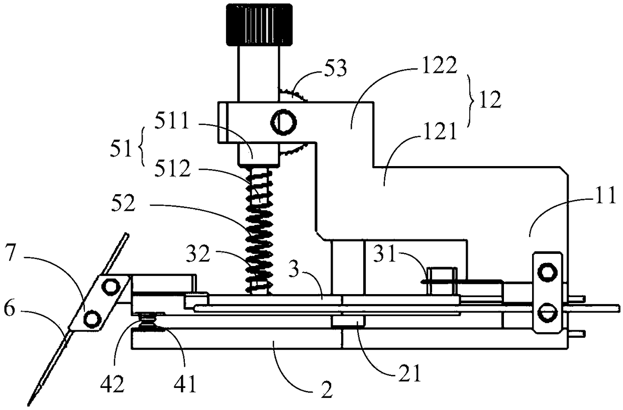
[0038] Reference will now be made in detail to the exemplary embodiments, examples of which are illustrated in the accompanying drawings. When the following description refers to the accompanying drawings, the same numerals in different drawings refer to the same or similar elements unless otherwise indicated. The implementations described in the following exemplary examples do not represent all implementations consistent with the present invention. Rather, they are merely examples of apparatuses and methods consistent with aspects of the invention as recited in the appended claims.

[0039] figure 1 is a perspective view of a power supply mechanism shown according to an exemplary embodiment, figure 2 It is a side view of the power supply mechanism shown according to an exemplary embodiment. The embodiment of the present invention provides a power supply mechanism, such as figure 1 , figure 2 As shown, the electrification mechanism includes: a base 1 , a static insulati...


PUM


Abstract

The invention provides a power-on mechanism, belonging to the chip test power-on technical field. The power-on mechanism comprises a base, a static insulating plate, a movable insulating plate, an elastic component, and a power-on probe. The base comprises a support part and a cantilever part. The static insulating plate is connected with the supporting part and has a first conductive sheet. The movable insulating plate is connected with the support part and has a second conductive sheet arranged opposite to the first conductive sheet. The movable insulating plate has a movement stroke relative to the static insulating plate so as to make the second conductive sheet come into contact with or separate from the first conductive sheet. The elastic component is connected with the cantilever part and abuts with the movable insulating plate in a force-adjustable manner, so that the first conductive sheet and the second conductive sheet are in contact with each other. The power-on probe is connected to an end of the second insulating plate remote from the support part. The power-on mechanism provided by the embodiment of the invention can provide protection to chips during the testing process, prevent the power-on probe from generating indentation on the chips, and ensure the chip quality.

Description

technical field [0001] The invention relates to the technical field of chip test power-on, in particular to a power-on mechanism. Background technique [0002] The semiconductor diode (Laser Diode, LD) chip is the core component of the semiconductor laser, which determines the luminous quality of the semiconductor laser. Therefore, in order to ensure the quality of semiconductor lasers, it is necessary to test and screen LD chips. Usually, the power-on probe is used as the power-on mechanism. When the power-on probe touches the LD chip, the LD chip is powered on and emits light, and then the screening is completed by testing the luminous quality of the LD chip. [0003] When the power-on mechanism provided in the related art is in use, it is difficult to sense whether the power-on probe has contacted the LD chip, resulting in excessive contact force between the power-on probe and the LD chip. In this case, for an LD chip with a thickness of 100 μm, it is very easy to leave...

Claims


Application Information

Patent Timeline
IPC IPC(8): G01R31/28
CPCG01R31/2806G01R31/2808
Inventor 陈玉梁
Owner HISENSE BROADBAND MULTIMEDIA TECH
Why Eureka
Try Eureka