a display device

A technology for a display device and a display area, which is applied to static indicators, instruments, optics, etc., and can solve problems such as affecting the performance of the display device and increasing light leakage current.

Active Publication Date: 2021-03-19
XIAMEN TIANMA MICRO ELECTRONICS
View PDF6 Cites 0 Cited by
  • Summary
  • Abstract
  • Description
  • Claims
  • Application Information

AI Technical Summary

Problems solved by technology

[0005] In view of this, the present invention provides a display device to solve the problem that the thin film transistor devices in the demultiplexer component DE-MUX and the test switch component VT SW located in the non-display area of ​​the array substrate in the prior art are easily affected by the backlight module. The impact of the high-brightness backlight leads to an increase in light leakage current, which affects the technical problems of the performance of the display device

Method used


Image

  • a display device
  • a display device
  • a display device

Examples


Embodiment Construction

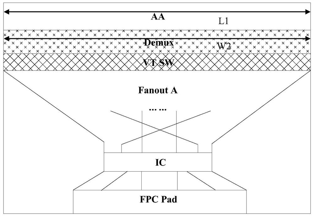
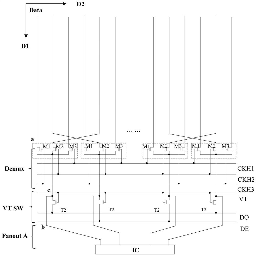
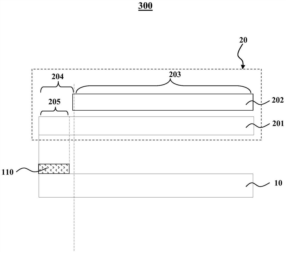
[0027] The specific implementation manners of the array substrate and the display device provided by the embodiments of the present invention will be described in detail below with reference to the accompanying drawings. The shapes and sizes of the elements in the drawings do not reflect the real proportion of the array substrate, but are only intended to schematically illustrate the content of the present invention.

[0028] figure 2 is a schematic diagram of the circuit structure of the array substrate in the prior art, image 3 It is a schematic cross-sectional structure diagram of a display device provided by an embodiment of the present invention. combine Figure 1-Figure 3 , the display device 300 includes a liquid crystal display panel 20 and a backlight module 10 located below the plane where the liquid crystal display panel 20 is located. Wherein, the liquid crystal display panel 20 includes an array substrate 201 and a color filter substrate 202 located above the...


PUM


Abstract

The invention discloses a display device, and the display device comprises an array substrate. The array substrate comprises a display area and a non-display area surrounding the display area, whereinthe non-display area comprises a light-shielding area, and also comprises a plurality of data signal sector lines, a demultiplexer component and a driving chip, which are respectively disposed in thenon-display area. The signal output end of the demultiplexer component is electrically connected with a plurality of data lines through the plurality of data signal sector lines, and the signal inputend of the demultiplexer component is electrically connected with the driving chip. The demultiplexer component is disposed at a side, far from the display area, of the plurality of data signal sector lines, and the spacing of adjacent first sub-thin film transistors of the demultiplexer component can be compressed in a second direction relative to a circuit structure in the prior art. The demultiplexer component is located in the light shielding area. In this way, the light leakage current of a transistor device in the demultiplexer component and / or a test switch component is reduced, and abetter display performance of the head-up display can be obtained.

Description

technical field [0001] The present invention relates to the field of display technology, and more specifically, to a display device. Background technique [0002] Head Up Display (HUD), referred to as HUD, is a comprehensive electronic display device used in automobiles or aircrafts. On the front windshield, the height is approximately at the level of the driver's eyes. When the driver looks forward through the HUD, he can easily integrate the external scene with the data displayed on the HUD, so that the driver can always keep his head up. Posture, reduce the delay and discomfort caused by ignoring the rapid changes in the external environment between raising and lowering the head and the need for constant adjustment of the eye focus. [0003] In existing display devices, the array substrate is an important part thereof. Generally, the array substrate includes a display area and a non-display area, and the display area is provided with data lines capable of controlling pi...

Claims


Application Information

Patent Timeline
Patent Type & Authority Patents(China)
IPC IPC(8): G02B27/01G02F1/13357G02F1/1362G02F1/1368G09G3/00
CPCG02B27/0101G02F1/133606G02F1/136286G02F1/1368G09G3/006
Inventor 吴薇赖国昌伍黄尧
Owner XIAMEN TIANMA MICRO ELECTRONICS
Why Eureka
Try Eureka