
Display panel and frame substrate thereof

A technology for display panels and substrates, which is applied to casings with display/control units, instruments, electrical components, etc., can solve problems such as frame substrate peeling, and achieve the effects of reducing extrusion force, reducing defects, and alleviating stress.

Inactive Publication Date: 2019-03-01
WUHAN CHINA STAR OPTOELECTRONICS TECH CO LTD
View PDF8 Cites 5 Cited by
  • Summary
  • Abstract
  • Description
  • Claims
  • Application Information

AI Technical Summary

Problems solved by technology

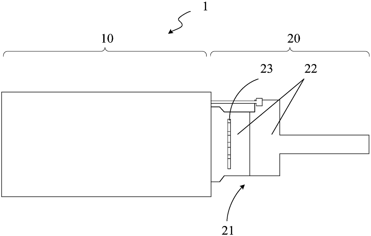
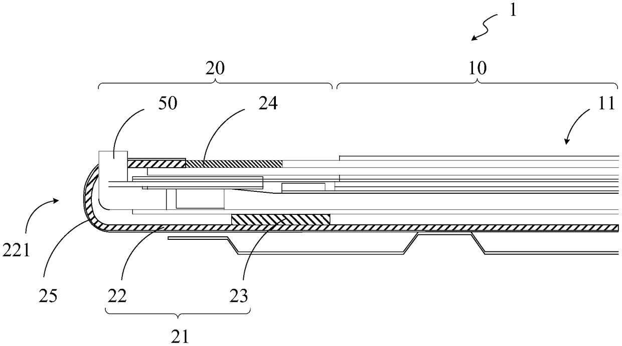
[0005] In view of this, the present invention provides a display panel and its frame substrate to solve the problem in the prior art that due to the strong rebound stress formed in the bending area after the frame substrate is folded back, this rebound stress makes this type of product often suffer from Defective phenomena such as peeling of the frame substrate from the display panel

Method used


Image

  • Display panel and frame substrate thereof
  • Display panel and frame substrate thereof
  • Display panel and frame substrate thereof

Examples


Embodiment Construction

[0033] The following descriptions of the various embodiments refer to the accompanying drawings to illustrate specific embodiments in which the present invention can be practiced. Furthermore, the directional terms mentioned in the present invention are, for example, up, down, top, bottom, front, back, left, right, inside, outside, side, surrounding, central, horizontal, transverse, vertical, longitudinal, axial, The radial direction, the uppermost layer or the lowermost layer, etc. are only directions referring to the attached drawings. Therefore, the directional terms used are used to illustrate and understand the present invention, but not to limit the present invention.

[0034] As used herein, the terms "comprising", "having" and their conjugations mean "including but not limited to".

[0035] As used herein, the terms "a", "an" and "at least one" include plural reference unless the context clearly dictates otherwise. For example, the term "a processing module" or "at l...


PUM


Abstract

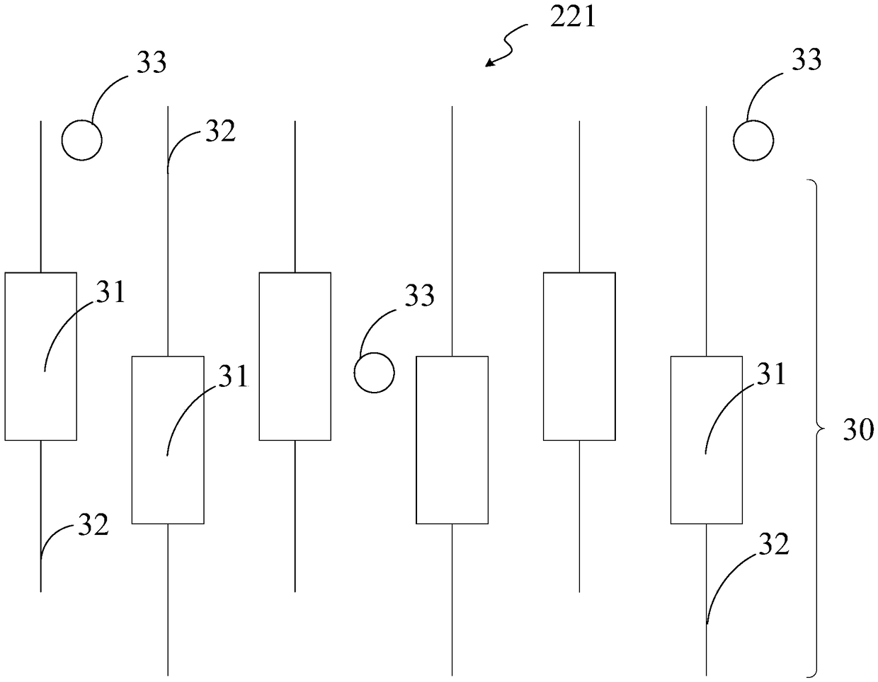
The invention provides a display panel and a frame substrate thereof. The frame substrate includes a bending area and a plurality of routing lines, each of the plurality of routing lines includes a first line area and a second line area, the first line area and the second line area are disposed on the bending area, and the width of the first line area of each of the plurality of routing lines is greater than the width of the second line area of the plurality of routing lines, and the first line areas of the adjacent routing lines are staggered from each other.

Description

technical field [0001] The invention relates to the field of liquid crystal display technology, in particular to a display panel with a chip-on-film package (COF). Background technique [0002] With the increasing demand for display devices, the requirements for display appearance are getting higher and higher, especially for mobile phone display products. The smaller the size, the better the display. [0003] In order to achieve a higher screen-to-body ratio, the glass adopts a chip-on-film package (COF, Chip On Film), that is, the chip is bound on a flexible circuit board (FPC, Flexible Printed Circuit) and folded to the back of the display substrate. package, thereby reducing the occupation of the glass substrate, and can shorten the lower frame of the small-sized display module to achieve a narrow frame, however, when the film-on-chip package is in an assembled state, the film-on-chip package has a One end of the upper part is bent to be installed under the display pan...

Claims


Application Information

Patent Timeline
Patent Type & Authority Applications(China)
IPC IPC(8): G09F9/30
CPCG09F9/301H05K1/028H05K2201/10128H05K2201/10136H05K1/189H05K2201/09236H05K2201/09727H05K2201/09709H05K2201/09063H05K1/0277H05K5/0017
Inventor 程艳
Owner WUHAN CHINA STAR OPTOELECTRONICS TECH CO LTD
Learn More