Rewiring structure for chip
A technology of re-wiring structure and re-wiring layer, applied in the direction of electrical components, electrical solid devices, circuits, etc., can solve the problems of complicated or even invalid metal pad connection, increase the test cost, etc., and achieve low cost, multiple selectivity, and use. handy effect
- Summary
- Abstract
- Description
- Claims
- Application Information
AI Technical Summary
Problems solved by technology
Method used
Image

Examples
Embodiment Construction
[0025] The present invention will be further described below in conjunction with the accompanying drawings and embodiments.
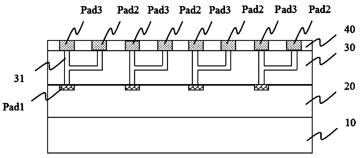
[0026] In a preferred embodiment, as figure 1 with figure 2 As shown, a chip rewiring structure is proposed, wherein it is applied to a chip 10 with a metal interconnection layer 20 formed on the upper surface, and a group of first metal pads are formed on the upper surface of the metal interconnection layer 20 pad1; the rewiring structure of the chip can include:
[0027] The redistribution layer 30 is formed with metal wiring 31;
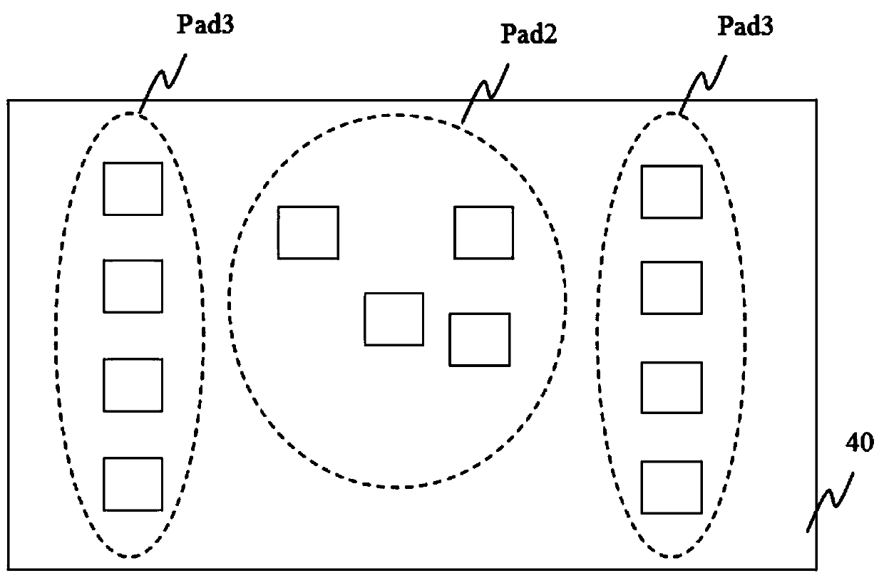
[0028] The pad layer 40 is formed on the upper surface of the redistribution layer, including a group of second metal pads pad2 and a group of third metal pads pad3;
[0029] There is at least one second metal pad pad2 connected to a first metal pad pad1 through a metal connection 31;
[0030] The number of the third metal pads pad3 is the same as that of the first metal pads pad1, and each third metal pad3 is respecti...
PUM
 Abstract
Description
Claims
Application Information
 - Generate Ideas
- Intellectual Property
- Life Sciences
- Materials
- Tech Scout
- Unparalleled Data Quality
- Higher Quality Content
- 60% Fewer Hallucinations
Browse by: Latest US Patents, China's latest patents, Technical Efficacy Thesaurus, Application Domain, Technology Topic, Popular Technical Reports.
© 2025 PatSnap. All rights reserved.Legal|Privacy policy|Modern Slavery Act Transparency Statement|Sitemap|About US| Contact US: help@patsnap.com