Semiconductor device and manufacturing method thereof

A manufacturing method and semiconductor technology, applied in semiconductor/solid-state device manufacturing, transistors, electrical components, etc., can solve the problem of high contact resistivity of PMOS, and achieve the effect of reducing source contact resistivity and/or drain contact resistivity

Active Publication Date: 2021-07-09
INST OF MICROELECTRONICS CHINESE ACAD OF SCI
View PDF6 Cites 0 Cited by
  • Summary
  • Abstract
  • Description
  • Claims
  • Application Information

AI Technical Summary

Problems solved by technology

[0004] The main purpose of this application is to provide a semiconductor device and its fabrication method to solve the problem of high contact resistivity of PMOS in the prior art

Method used


Image

  • Semiconductor device and manufacturing method thereof
  • Semiconductor device and manufacturing method thereof
  • Semiconductor device and manufacturing method thereof

Examples


Embodiment

[0048] A method of fabricating a semiconductor device includes:

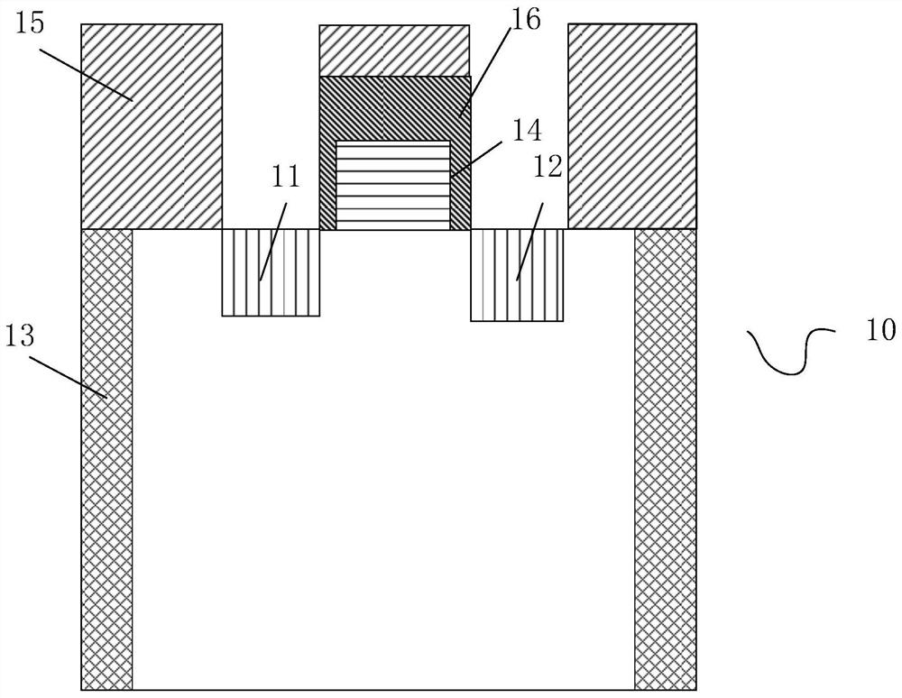
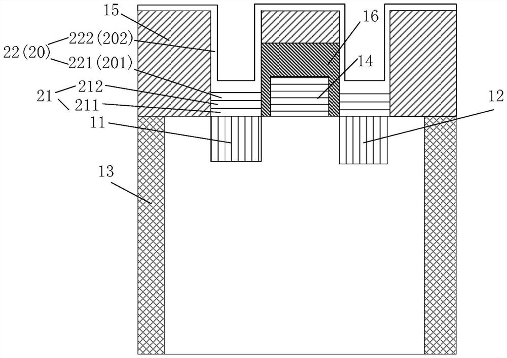
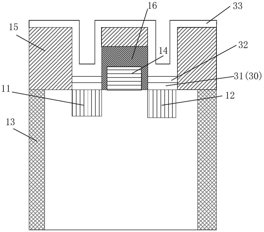
[0049] Such as figure 1 As shown, a semiconductor preparation 10 is provided, and the semiconductor preparation 10 includes a substrate, a shallow trench isolation 13 located in the substrate, a source region 11 and a drain region 12 located in the substrate, above and between the source and drain regions Between the gate 14, the sidewall layer 16 on the surface of the gate 14, and the isolation dielectric layer 15 above the substrate and on both sides of the source and drain regions and on the sidewall layer 16. Wherein, a through hole is formed between the isolation dielectric layer 15 and the side wall layer 16 . The substrate is a Si substrate, the source and drain regions are GeSi source and drain regions doped with B, the gate 14 is a high-K gate, the sidewall layer 16 is a silicon dioxide layer, and the isolation dielectric layer 15 is a silicon dioxide layer. It should be noted, figure 1 For the con...


PUM

PropertyMeasurementUnit
electron work functionaaaaaaaaaa
thicknessaaaaaaaaaa

Abstract

The application provides a semiconductor device and a manufacturing method thereof. The method includes: providing a semiconductor preparation having a source region and a drain region; and sequentially stacking at least two gold half-units on the exposed surface of the source region and / or the drain region, and each gold half-unit is along a direction away from the semiconductor preparation It includes a semiconductor layer and a metal layer in turn, wherein the material of each semiconductor layer is independently selected from GeSi, Si or Ge, among the plurality of gold half-units, the gold half-unit with the smallest distance from the semiconductor preparation is the first gold half-unit, The first gold half-unit includes a first semiconductor layer and a first metal layer, and the work function of the metal of the first metal layer is smaller than that of other metal layers; heat treatment is carried out to the semiconductor preparation provided with a plurality of gold half-units, so that At least part of the material of the semiconductor layer reacts with part of the material of the adjacent metal layer to form at least three metal-semiconductor compound layers. The resistance of the semiconductor device manufactured by the manufacturing method is small.

Description

technical field [0001] The present application relates to the field of semiconductors, and in particular, to a semiconductor device and a manufacturing method thereof. Background technique [0002] As the CMOS technology generation enters the technology node of 16 / 14nm and below, the contact resistance of the source and drain regions plays a vital role in the improvement of device performance. Traditional CMOS devices usually only use one kind of metal silicide, and it is difficult to make N / P MOS form low contact resistivity at the same time. Moreover, due to the solid concentration limitation of impurity B in the source and drain of germanium and silicon, compared with NMOS, the contact resistance of PMOS is reduced rate is more challenging. [0003] The above information disclosed in the Background section is only to enhance the understanding of the background of the technology described herein, therefore, the Background may contain certain information which is not forme...

Claims


Application Information

Patent Timeline
Patent Type & Authority Patents(China)
IPC IPC(8): H01L21/8238H01L27/092
CPCH01L21/823871H01L27/092
Inventor 毛淑娟罗军许静
Owner INST OF MICROELECTRONICS CHINESE ACAD OF SCI
Why Eureka
Try Eureka