
Element sealing body and method for producing the same

A manufacturing method and sealing body technology, which are applied in semiconductor/solid-state device manufacturing, electrical components, electric solid-state devices, etc., can solve the problems of destroying substrate light-emitting elements, light-emitting elements not resistant to high heat, and insufficient gas shielding properties of sealants, etc. Achieve strong sealing, excellent tightness, and excellent gas barrier effect

Inactive Publication Date: 2015-04-01
NIPPON ELECTRIC GLASS CO LTD
View PDF6 Cites 0 Cited by
  • Summary
  • Abstract
  • Description
  • Claims
  • Application Information

AI Technical Summary

Problems solved by technology

However, when a resin-based sealant described in the following Patent Document 1 is used for bonding glass substrates, the gas barrier properties of the sealant may not be sufficient. Or gas such as water vapor permeates the resin sealant and enters the inside, which will cause aging degradation of the light-emitting element
[0005] However, since the light-emitting elements used in organic EL displays are not resistant to high heat, when using the glass frit composition described in Patent Document 2 below, the high-temperature sintering process at 700°C may damage the light-emitting elements in the substrate

Method used

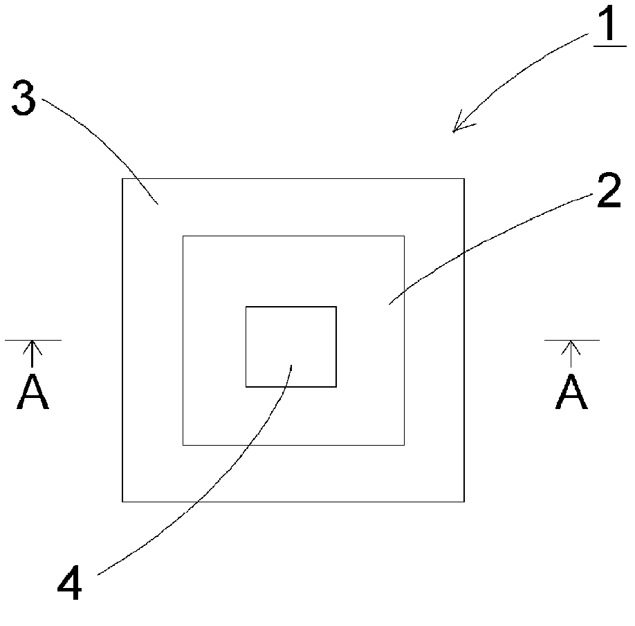
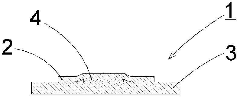
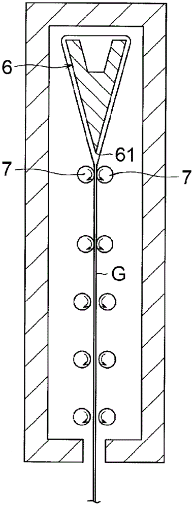

Image

  • Element sealing body and method for producing the same
  • Element sealing body and method for producing the same
  • Element sealing body and method for producing the same

Examples


Embodiment 1

[0064] Hereinafter, although the element sealing body of this invention is demonstrated in detail based on an Example, this invention is not limited to these Examples.

[0065] A rectangular transparent glass plate having a length of 100 mm, a width of 100 mm, and a thickness of 700 μm was used as a substrate glass. As the cover glass laminated on the substrate glass, a cover glass with a length of 80 mm, a width of 80 mm, and a thickness of 100 μm was used. The substrate glass and cover glass use alkali-free glass manufactured by NEC Glass Co., Ltd. (product name: OA-10G, coefficient of thermal expansion at 30 to 380°C: 38×10 -7 / °C). The glass formed by the overflow down-draw method is used in an unpolished state, or the surface roughness Ra is controlled by appropriately controlling the amount of grinding and chemical etching. Using AFM (Nanoscope III a) manufactured by Veeco, under conditions of a scan size of 10 μm, a scan frequency of 1 Hz, and a sample line of 512, th...


PUM

PropertyMeasurementUnit
surface roughnessaaaaaaaaaa
thicknessaaaaaaaaaa
thicknessaaaaaaaaaa

Abstract

An element sealed body comprises a glass substrate, an element mounted on the glass substrate, and a protective glass for sealing the element, wherein a surface of the protective glass and a surface of the glass substrate, which are brought into contact with each other, have a surface roughness Ra of 2.0 nm or less respectively.

Description

technical field [0001] This invention relates to the element sealing body which seals the element used for flat panel displays, such as a liquid crystal display and an organic electroluminescent display, using glass. Background technique [0002] From the viewpoint of saving space, flat panel displays such as liquid crystal displays, plasma displays, organic EL displays, and field emission displays have become popular in recent years instead of conventional CRT displays. Organic EL displays, which are difficult to increase in size and are becoming popular as displays for small devices such as mobile phones, have a faster response speed and a better viewing angle than liquid crystal displays, and consume less power than plasma displays, so they are expected to be used as large-screen TVs. Mass production, companies are currently developing towards large-scale screens. [0003] A light-emitting element used in an organic EL display deteriorates due to contact with gas such as...

Claims


Application Information

Patent Timeline
Patent Type & Authority Patents(China)
IPC IPC(8): C03C27/06H01L51/50H05B33/04
CPCC03C27/06Y10T428/239Y10T428/23H05B33/04H01L51/5237H10K50/80H10K50/841H10K50/8426H10K50/84
Inventor 高谷辰弥泷本博司
Owner NIPPON ELECTRIC GLASS CO LTD
Learn More