Automatic silicon wafer sorting equipment

An automatic sorting and silicon wafer technology, applied in sorting and other directions, can solve problems such as single detection parameters, high false detection rate, and low production efficiency, and achieve the effects of reducing false detection rate, accurate sorting, and improving production capacity

Pending Publication Date: 2019-04-02
TIANJIN HUANXIN TECH DEV
View PDF8 Cites 5 Cited by
  • Summary
  • Abstract
  • Description
  • Claims
  • Application Information

AI Technical Summary

Problems solved by technology

[0011] The purpose of the present invention is to provide an automatic sorting device for silicon wafers, to solve the problems of low production efficiency, high false detection rate and single detection parameters in the prior art

Method used


Image

  • Automatic silicon wafer sorting equipment
  • Automatic silicon wafer sorting equipment
  • Automatic silicon wafer sorting equipment

Examples


Embodiment Construction

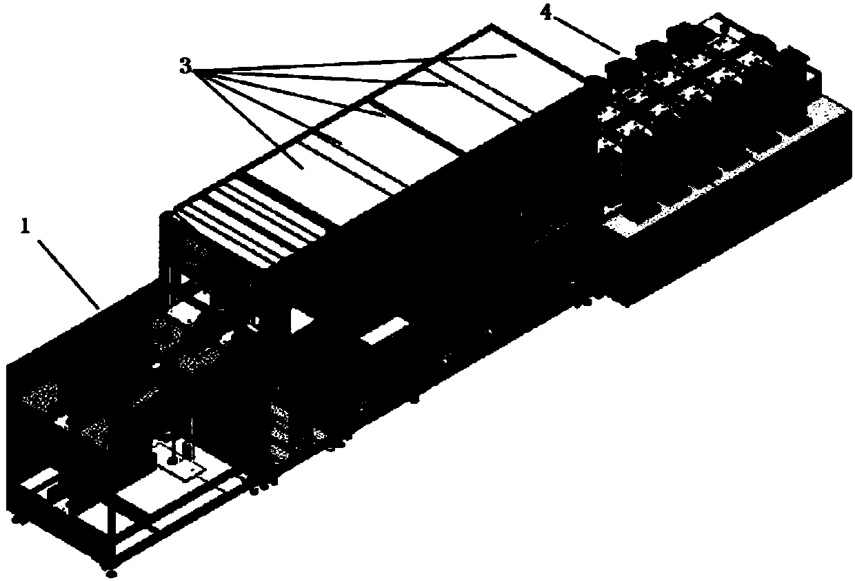
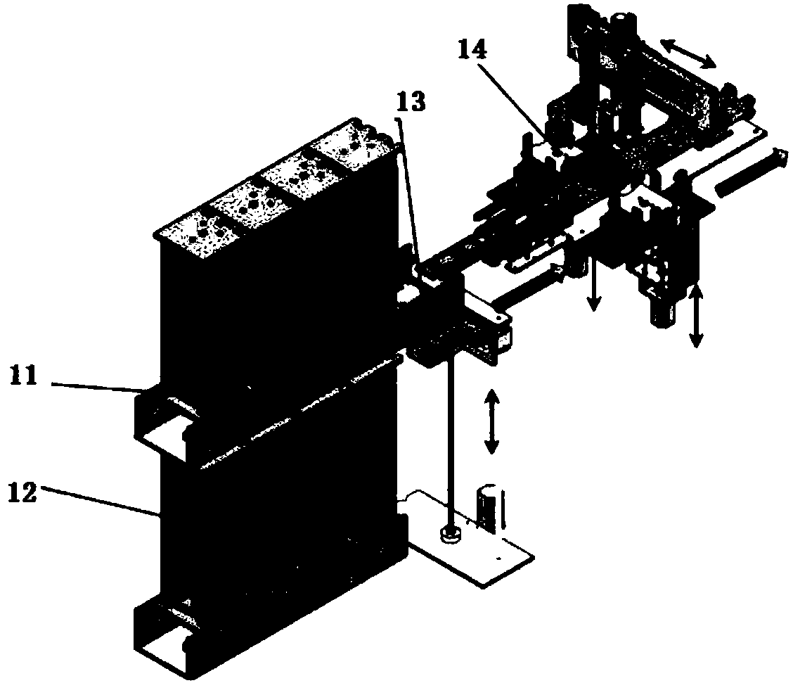
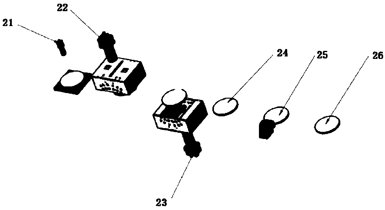
[0041] Such as Figure 1-4 As shown, this example is an automatic sorting device for silicon wafers, including a feeding part 1, a detection part 2 and a feeding part 3 arranged in sequence, and the detection part 2 includes a transmission mechanism, a positioning mechanism 21, a surface detection module, and a geometric parameter detection Module 24 and resistivity detection module 25, wherein, the transmission mechanism is arranged in the detection part 2, and the transmission mechanism adopts a belt transmission line, and the belt transmission line runs through the detection part for transmitting the silicon wafer; the positioning mechanism 21 is arranged at the starting point of the transmission mechanism At the beginning, the silicon wafers in the basket are positioned; the surface detection module includes an upper surface detection module 22 and a lower surface detection module 23, which are arranged on the side and top of the transmission mechanism to detect appearance ...


PUM


Abstract

The invention provides automatic silicon wafer sorting equipment. The equipment comprises a feeding part, a detecting part and a discharging part which are sequentially arranged; the detecting part comprises a transmission mechanism, a positioning mechanism, surface detecting modules, a geometric parameter detecting module and a resistivity detecting module, wherein the transmission mechanism is arranged in the detecting part and used for transmitting silicon wafers; the positioning mechanism is arranged at the starting end of the transmission mechanism, and is used for positioning dischargedsilicon wafers from wafer discharging baskets; the surface detecting modules are arranged on the side surface and the upper surface of the transmission mechanism and used for detecting the appearancedefects of the surface of the silicon wafer; the geometric parameter detecting module is arranged in the detecting part and used for measuring the thickness of the silicon wafer; and the resistivity detecting module is arranged in the detecting part and used for measuring the electric loss of the silicon wafer. The equipment has the beneficial effects that a belt transmission line, the appearancedetecting, the geometrical parameter detecting, the resistivity detecting, the laser marking and other functions are integrated, so that automatic, efficient and accurate sorting of the silicon waferis realized, the capacity of silicon wafer detecting sorting is effectively improved, the silicon wafer is guaranteed to be sorted freely according to resistivity, thickness, appearance and other parameters, and the false detecting rate can be reduced.

Description

technical field [0001] The invention belongs to the technical field of semiconductor silicon wafer production machinery, and in particular relates to an automatic sorting equipment for silicon wafers. Background technique [0002] Semiconductor silicon wafers are the basic raw materials for the manufacture of semiconductor devices. The semiconductor device production line produces many products with different specifications and models. According to the specifications of different devices, silicon wafers with specific resistivity and thickness need to be selected for production. If the resistivity, thickness and appearance of the selected silicon wafer do not meet the requirements, the produced product will deviate from the electrical parameters, resulting in defective products. At present, the parameters to be tested for incoming silicon wafers are as follows: [0003] 1. Wafer appearance parameters: edge chipping, notch, stain, scratch; [0004] 2. Wafer geometric param...

Claims


Application Information

Patent Timeline
Patent Type & Authority Applications(China)
IPC IPC(8): B07C5/10B07C5/344B07C5/342B07C5/02B07C5/36
CPCB07C5/02B07C5/10B07C5/342B07C5/344B07C5/362B07C2301/0008
Inventor 齐风甄辉徐艳超徐长坡陈澄梁效峰杨玉聪李亚哲黄志焕王晓捧王宏宇王鹏
Owner TIANJIN HUANXIN TECH DEV
Why Eureka
Try Eureka