
OLED (Organic Light Emitting Diode) display device and manufacture method thereof

A technology for a display device and a manufacturing method, applied in static indicators, final product manufacturing, sustainable manufacturing/processing, etc., capable of solving problems such as disconnection and occupancy, achieving increased screen-to-body ratio, reduced border width, and reduced disconnection risk effect

Active Publication Date: 2019-04-09
WUHAN CHINA STAR OPTOELECTRONICS SEMICON DISPLAY TECH CO LTD
View PDF5 Cites 8 Cited by
  • Summary
  • Abstract
  • Description
  • Claims
  • Application Information

AI Technical Summary

Problems solved by technology

[0005] With the development of science and technology and the improvement of people's requirements for products, while OLED display devices are pursuing high resolution, they are also continuously increasing the screen-to-body ratio, and the narrow bezel technology has also been developed rapidly. From the original chip on film (Chip On Film, COF) bonding, it has gradually developed into a bending (bending) bonding structure. Specifically, the bonding terminal is formed on the substrate, and the flexible circuit board is bonded. After being fixed on the binding terminal, it is bent to the back of the substrate to increase the screen-to-body ratio. In practical applications, the bending radius of the flexible circuit board is getting smaller and smaller, and the frame of the display panel is also getting smaller. However, due to the wiring structure Limitation, the bending radius needs to be kept within a certain range in practical application, and it cannot be infinitely small. It always needs to occupy a certain frame width, because it is easy to cause broken wires when bending

Method used


Image

  • OLED (Organic Light Emitting Diode) display device and manufacture method thereof
  • OLED (Organic Light Emitting Diode) display device and manufacture method thereof
  • OLED (Organic Light Emitting Diode) display device and manufacture method thereof

Examples


Embodiment Construction

[0041] In order to further illustrate the technical means adopted by the present invention and its effects, the following describes in detail in conjunction with preferred embodiments of the present invention and accompanying drawings.

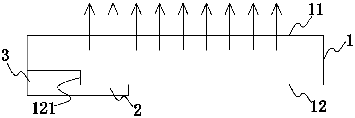
[0042] see Figure 1 to Figure 3 , the present invention provides an OLED display device, comprising: an OLED display panel 1, a driving module 2 and a binding terminal 3;

[0043] The OLED display panel 1 has a light-emitting surface 11 and a non-light-emitting surface 12 opposite to the light-emitting surface 11, the binding terminal 3 is arranged on the non-light-emitting surface 12, and the driving module 2 is bound to the Bind to terminal 3 as described above.

[0044] Specifically, such as Figure 4 or Figure 8 As shown, the OLED display panel 1 includes a flexible substrate 10, a driving circuit layer 20 disposed on the flexible substrate 10, an OLED layer 30 disposed on the driving circuit layer 20, and an OLED layer disposed on th...


PUM


Abstract

The invention provides an OLED (Organic Light Emitting Diode) display device and a manufacture method thereof. The OLED display device comprises an OLED display panel, a driving module and a binding terminal, wherein the OLED display panel is provided with a light emitting surface and a non-light-emitting surface opposite to the light emitting surface; the binding terminal is arranged on the non-light-emitting surface; the driving module is bound to the binding terminal; the binding terminal is arranged on the non-light-emitting surface of the OLED display panel; and the driving module is bound to the binding terminal of the non-light-emitting surface. Compared with the prior art, the OLED display device is characterized in that: since the binding terminal is positioned on the non-light-emitting surface of the OLED display panel, the bound driving module does not need to be bent, so that border width is reduced to a maximum degree, and a line breaking risk is lowered while a screen-to-body ratio is improved.

Description

technical field [0001] The invention relates to the field of display technology, in particular to an OLED display device and a manufacturing method thereof. Background technique [0002] With the development of display technology, flat panel display devices are widely used in mobile phones, televisions, personal digital assistants, digital cameras, notebook computers, desktops, etc. Various consumer electronic products such as computers have become the mainstream of display devices. [0003] Organic Light Emitting Display (OLED) has self-illumination, no backlight, high contrast, thin thickness, wide viewing angle, fast response, can be used for flexible panels, wide operating temperature range, structure It is considered to be an emerging application technology for the next generation of flat panel displays due to its excellent characteristics such as simple manufacturing process. [0004] OLED display devices generally include: a substrate, an anode disposed on the subst...

Claims


Application Information

Patent Timeline
Patent Type & Authority Applications(China)
IPC IPC(8): H01L27/32H01L51/52
CPCH10K59/123H10K59/1213H10K59/131H10K59/873H10K71/00Y02E10/549Y02P70/50H10K77/111H10K2102/311G09G3/3225H10K50/84H10K2102/3026
Inventor 胡妞
Owner WUHAN CHINA STAR OPTOELECTRONICS SEMICON DISPLAY TECH CO LTD
Learn More