Security testing method of encryption chip based on scanning obfuscation

An encryption chip and chip technology, which is applied in the direction of measuring electricity, measuring devices, measuring electrical variables, etc., can solve the problems of not finding a patented invention of encryption chip security testing method, and achieve high security performance, low area cost, and small area cost. Effect

Inactive Publication Date: 2021-08-17
CHANGSHA UNIVERSITY OF SCIENCE AND TECHNOLOGY
View PDF8 Cites 0 Cited by
  • Summary
  • Abstract
  • Description
  • Claims
  • Application Information

AI Technical Summary

Problems solved by technology

[0005] Among the existing patents, no patented invention similar to the encryption chip security testing method based on scanning confusion was found

Method used


Image

  • Security testing method of encryption chip based on scanning obfuscation

Examples


Embodiment Construction

[0017] The present invention will be described in detail below in conjunction with the accompanying drawings.

[0018] In order to make the object, technical solution and advantages of the present invention clearer, the present invention will be further described in detail below in conjunction with the accompanying drawings and embodiments. It should be understood that the specific embodiments described here are only used to explain the present invention, not to limit the present invention.

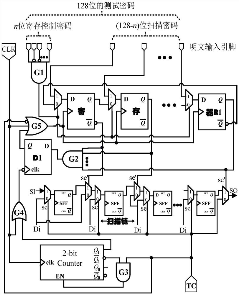
[0019] Such as figure 1 As shown, the security scanning scheme of the present invention can be by adding scanning password register (R1), confusing data selector, a 2-bit counter, a D flip-flop (D1) and a small number of logic gates on the basis of conventional scanning structure (G1 ~ G5) to achieve. For block-based encryption algorithms (such as AES encryption algorithm), its hardware implementation includes at least 128-bit plaintext input. When the chip enters the test mode for the...


PUM


Abstract

The invention relates to a testability design structure based on scanning confusion and protecting encryption chips from scanning attacks. On the basis of the conventional scan design structure, the secure testability design structure introduces the scan password register and related logic, requiring the test password to be loaded from the chip input port first during testing. Only when the correct test password is loaded, the chip test can be performed normally. If the attacker does not understand the correct test process and does not have the correct test password, then he cannot load the correct test password through a specific input port within the specified time, so that in 1‑2 ‑128 It is impossible to scan any value for the scan chain under the probability of , and the real state of the scan chain cannot be observed from the output terminal. It is actually impossible to conduct non-invasive attacks based on scanning. The invention resists the existing scan-based non-invasion attack without affecting the circuit performance and test quality and without increasing the test time.

Description

technical field [0001] The invention belongs to the field of hardware safety, and more specifically relates to a safety test structure for protecting an encryption chip from scanning attacks. Background technique [0002] With the development of information and digital society, information security and confidentiality have become more and more important, and encryption algorithms have been widely used. Regardless of high-end security processors or low-end smart cards, in order to improve data throughput, encryption algorithms are usually implemented using hardware modules. Cryptographic algorithms have zero tolerance for errors, so cryptographic hardware needs to be rigorously tested. [0003] Scan design is a widely used testability design technology for integrated circuits. It enhances the testability of circuits by directly controlling and observing the state of internal flip-flops, and converts the test problems of sequential circuits into test problems of combinational...

Claims


Application Information

Patent Timeline
Patent Type & Authority Patents(China)
IPC IPC(8): G01R31/3185
CPCG01R31/318544G01R31/318586G01R31/318588
Inventor 王伟征王威蔡烁
Owner CHANGSHA UNIVERSITY OF SCIENCE AND TECHNOLOGY
Why Eureka
Try Eureka