Display panel, manufacturing method thereof, and display device
A technology for display panels and substrates, applied in optical components, instruments, optics, etc., can solve the problems of high material requirements for common electrodes and achieve the effect of low manufacturing requirements
- Summary
- Abstract
- Description
- Claims
- Application Information
AI Technical Summary
Problems solved by technology
Method used
Image

Examples
Embodiment Construction
[0059] In order to make the purpose, technical solution and advantages of the present application clearer, the implementation manners of the present application will be further described in detail below in conjunction with the accompanying drawings.
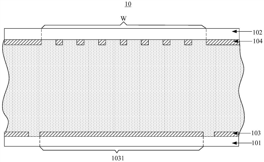
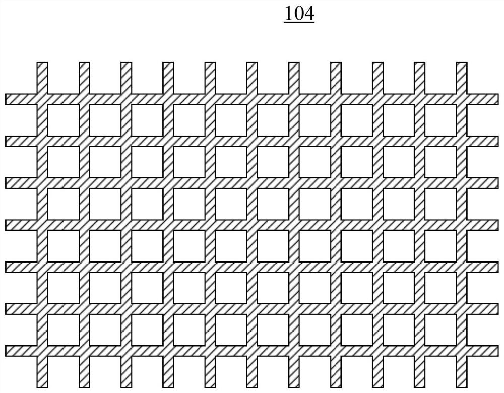
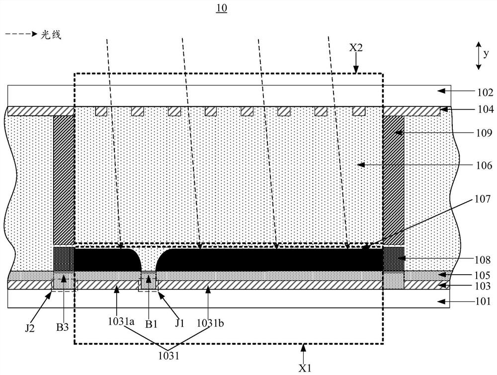
[0060] With the development of display technology, how to reduce the manufacturing requirements for each film layer in the display panel and reduce the manufacturing cost of the display panel has become a hot research direction. Generally, each film layer in the display panel needs to have different characteristics, for example, the common electrode in the display panel needs to be transparent and conductive, and when the display panel is a flexible display panel, the common electrode needs to be flexible. In order for the common electrode to have these various characteristics, the material requirements for the common electrode are relatively high, and usually the cost of the material having these various characteristics is relati...
PUM
 Abstract
Description
Claims
Application Information
 - R&D
- Intellectual Property
- Life Sciences
- Materials
- Tech Scout
- Unparalleled Data Quality
- Higher Quality Content
- 60% Fewer Hallucinations
Browse by: Latest US Patents, China's latest patents, Technical Efficacy Thesaurus, Application Domain, Technology Topic, Popular Technical Reports.
© 2025 PatSnap. All rights reserved.Legal|Privacy policy|Modern Slavery Act Transparency Statement|Sitemap|About US| Contact US: help@patsnap.com