Integrated circuit layout method and distributed design method

A technology of integrated circuits and layout methods, applied in computing, electrical digital data processing, special data processing applications, etc., can solve problems such as low efficiency, and achieve the effect of efficient layout solutions

Pending Publication Date: 2019-04-16
CHENGDU SINO MICROELECTRONICS TECH CO LTD
View PDF9 Cites 0 Cited by
  • Summary
  • Abstract
  • Description
  • Claims
  • Application Information

AI Technical Summary

Problems solved by technology

The designs of existing technologies all rely on manual changes and optimized design solutions, which is very inefficient

Method used


Image

  • Integrated circuit layout method and distributed design method
  • Integrated circuit layout method and distributed design method
  • Integrated circuit layout method and distributed design method

Examples


Embodiment

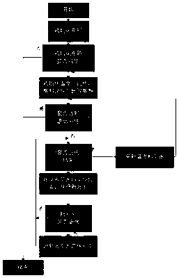
[0061] 1) The server side reads the logical netlist that needs to be laid out, and generates graph G logic (V logic ,E logic ), where the set of vertices V logic Each element in is a layoutable logical unit, which contains information such as the name, type, and constraints of the logical unit. The edge set E logic Contains associations between logical units.

[0062] 2) The server reads the integrated circuit chip model library file and generates graph G device (V device ,E device ), where the set of vertices V device Each element in is an available layout unit, including the name, type, location and other related information of the unit. The edge set E device Contains the association relationship between physical resources. It is initially empty and is constantly modified during the layout process. device .

[0063] 3) The layout is for V logic Each logic cell in is assigned a corresponding V device In the physical unit, at the same time need to consider how to me...


PUM


Abstract

The invention discloses an integrated circuit layout method and a distributed design method, and relates to an integrated circuit technology. The integrated circuit layout method comprises the following steps: 1) layout scheme arrangement: determining the format of a layout scheme according to the distribution of a logic netlist and physical units, each layout scheme comprising a characteristic value part and the cost value of the layout scheme, and the characteristic value part comprising a logic block connection relation matrix and a logic block position vector; and 2) generating a layout scheme by adopting an annealing algorithm, and optimally selecting the layout scheme with the lowest cost as an optimal solution. According to the invention, the optimal layout scheme can be formed in an efficient manner.

Description

technical field [0001] The present invention relates to integrated circuit technology. Background technique [0002] The layout tool in integrated circuit design is to allocate a reasonable integrated circuit chip hardware resource for each instance in the logic netlist. Suppose we have a simple logic netlist, there are six logic blocks A, B, C, D, E and F of the same type, the connection relationship between the logic blocks is as follows figure 1 ; There is a simple device model with 20 (4x5) physical cells that can be used to place logic blocks. Matching the logic block to the physical unit will generate a layout scheme, connect the used physical units according to the connection relationship according to the logic netlist, and use the slice spacing to measure the cost of the layout scheme. Now suppose a layout scheme S1 is generated such as figure 2 , the cost of the scheme is as image 3 , with a total cost of 22. Now we place E on the last physical unit in the se...

Claims


Application Information

Patent Timeline
Patent Type & Authority Applications(China)
IPC IPC(8): G06F17/50
CPCG06F30/392G06F2115/06G06F30/398
Inventor 鞠瑜华白利琼赵剑峰
Owner CHENGDU SINO MICROELECTRONICS TECH CO LTD
Why Eureka
Try Eureka