
Display processing method and display processing device of a display panel

A display processing method and display panel technology, applied to static indicators, instruments, etc., can solve problems such as inability to achieve high PPI, low accuracy of coefficients, and large limitations, so as to improve image display effects, eliminate mura, and enhance Feasibility effect

Active Publication Date: 2020-07-24
XIAMEN TIANMA MICRO ELECTRONICS
View PDF12 Cites 0 Cited by
  • Summary
  • Abstract
  • Description
  • Claims
  • Application Information

AI Technical Summary

Problems solved by technology

Consumers cannot accept poor display of the display panel, for example: mura (moiré)
At present, there are mainly three methods to solve the problem of poor display: 1. The compensation method of TFT circuit often needs to design a more complex pixel circuit to realize the compensation of the threshold deviation of the TFT tube. The complex circuit structure increases the difficulty of technical realization and limits The area of ​​the light-emitting area is limited, so it is impossible to achieve high PPI; 2. For external voltage and current compensation, peripheral circuits must be designed to monitor the voltage or current of the pixel, and the cooperation of the panel is required to pull out the signal for monitoring , which increases the complexity of the circuit, which is not conducive to achieving narrow borders; 3. The existing optical compensation schemes are all based on gray scales to adjust the uneven light emission between pixels, and gray scales are very important for the driver IC (Driver IC) and For OLED display devices, it is a relative concept, depending on the relationship between grayscale, voltage and brightness set by the gamma curve, the grayscale is changed to a preset voltage value through the Driver IC to achieve Driving the OLED display device to emit light can complete the adjustment of uneven brightness between pixels, but when the gamma curve changes, such as when the display device uses high-brightness mode, power-saving mode, etc., the accuracy of mura elimination cannot be guaranteed. Limitations bigger
In addition, the coefficients stored in the existing optical compensation schemes are all parameters to be corrected, because the correction parameters of different gray scales are different, and no memory chip (flash IC) can store all the correction parameters of 0-255 gray scales. , so the usual practice is to store a few specific grayscale correction parameters, and the rest of the grayscales are calculated by interpolation. Often the coefficients obtained by this method are not very accurate, and the final compensation effect will also be biased.

Method used


Image

  • Display processing method and display processing device of a display panel
  • Display processing method and display processing device of a display panel
  • Display processing method and display processing device of a display panel

Examples


Embodiment Construction

[0022] In order to better understand the technical solutions of the present invention, the embodiments of the present invention will be described in detail below with reference to the accompanying drawings.

[0023] It should be clear that the described embodiments are only a part of the embodiments of the present invention, rather than all the embodiments. Based on the embodiments of the present invention, all other embodiments obtained by those of ordinary skill in the art without creative work shall fall within the protection scope of the present invention.

[0024] The terms used in the embodiments of the present invention are only for the purpose of describing specific embodiments, and are not intended to limit the present invention. The singular forms of "a", "said" and "the" used in the embodiments of the present invention and the appended claims are also intended to include plural forms, unless the context clearly indicates other meanings.

[0025] It should be understood th...


PUM


Abstract

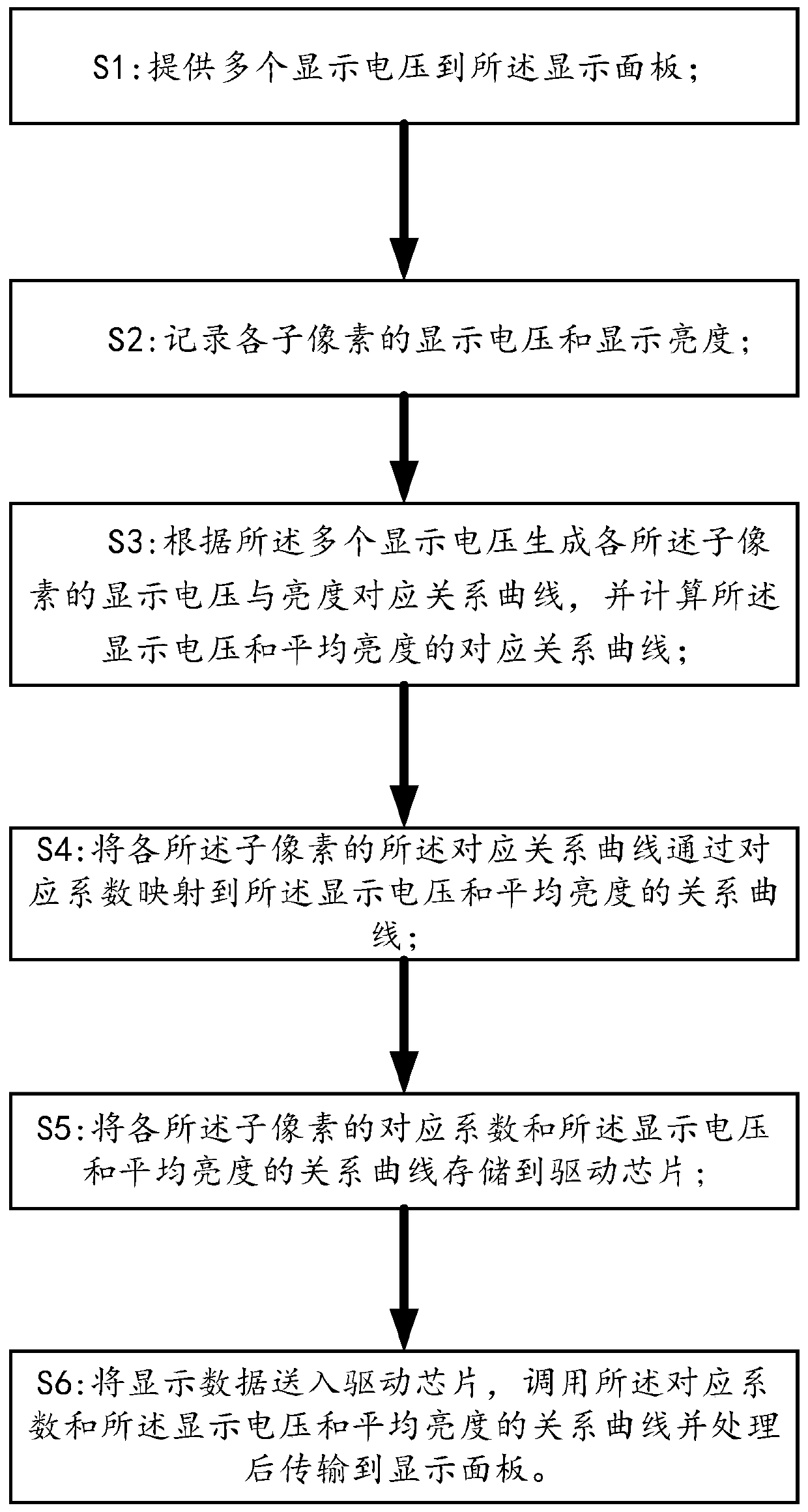
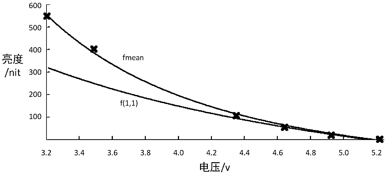
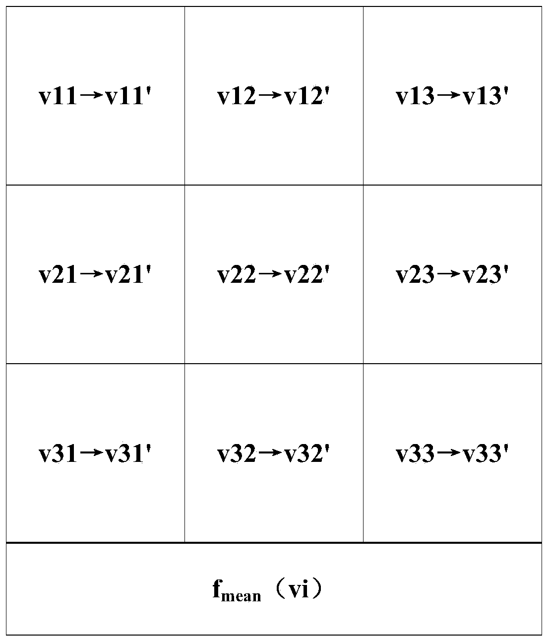
The embodiments of the invention provide a display panel. Display voltages and display brightness of each subpixel are recorded. A display voltage and brightness relationship curve of each subpixel isgenerated according to a plurality of display voltages. A relationship curve between the display voltages and average brightness is computed. The relationship curve of each subpixel is mapped to therelationship curve between the display voltages and the average brightness through utilization of a corresponding coefficient. The corresponding coefficient of each pixel and the relationship curve between the display voltages and the average brightness are stored to a drive chip. Display data is sent to the drive chip. The corresponding coefficient and the relationship curve between the display voltages and the average brightness are called, processed and then are transmitted to the display panel. According to the display panel, mura of each gray scale can be eliminated, and an image displayeffect can be improved both in a low brightness mode and a high brightness mode.

Description

【Technical Field】 [0001] The present invention relates to the field of display technology, and in particular to a display processing method and display processing device of a display panel. 【Background technique】 [0002] With the rapid development of display technology, consumers have increasingly higher requirements for display effects of display devices. Consumers cannot accept poor display of the display panel, such as mura (moire). At present, there are three main methods for solving poor display: 1. Compensation methods for TFT circuits, often need to design more complex pixel circuits to achieve compensation for the threshold deviation of TFT tubes. The complex circuit structure increases the difficulty and limits of the process. Because of the area of ​​the light-emitting area, high PPI cannot be achieved; 2. For external voltage and current compensation, peripheral circuits must be designed to monitor the voltage or current of the pixels, and the internal cooperation of...

Claims


Application Information

Patent Timeline
Patent Type & Authority Patents(China)
IPC IPC(8): G09G3/3208G09G3/20
CPCG09G3/2074G09G3/3208G09G2320/0626
Inventor 边青吕博嘉孔祥梓
Owner XIAMEN TIANMA MICRO ELECTRONICS
Learn More