Systems with multiple layers of semiconductor x-ray detectors
An X-ray and detector technology, applied in the field of packaged semiconductor X-ray detectors, can solve the problems of difficult and impossible production of detectors with large areas and a large number of pixels
- Summary
- Abstract
- Description
- Claims
- Application Information
AI Technical Summary
Problems solved by technology
Method used
Image
Examples
Embodiment Construction
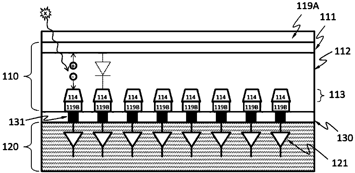
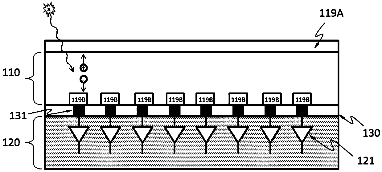
[0069] Figure 1A A cross-sectional view of a detector 100 according to an embodiment is schematically shown. The detector 100 may include an X-ray absorbing layer 110 and an electronic layer 120 (for example, an ASIC) for processing or analyzing electrical signals generated in the X-ray absorbing layer 110 by incident X-rays. In an embodiment, detector 100 does not include a scintillator. The X-ray absorbing layer 110 may include semiconductor materials such as silicon, germanium, GaAs, CdTe, CdZnTe or combinations thereof. Semiconductors can have high mass attenuation coefficients for x-ray energies of interest.
[0070] as in Figure 1B As shown in the detailed cross-sectional view of the detector 100, according to an embodiment, the X-ray absorbing layer 110 may include one or more discrete regions 114 formed by the first doped region 111, the second doped region 113 One or more diodes (eg, p-i-n or p-n). The second doped region 113 may be separated from the first dope...
PUM
| Property | Measurement | Unit |
|---|---|---|
| thickness | aaaaa | aaaaa |
Abstract
Description
Claims
Application Information
 - R&D Engineer
- R&D Manager
- IP Professional
- Industry Leading Data Capabilities
- Powerful AI technology
- Patent DNA Extraction
Browse by: Latest US Patents, China's latest patents, Technical Efficacy Thesaurus, Application Domain, Technology Topic, Popular Technical Reports.
© 2024 PatSnap. All rights reserved.Legal|Privacy policy|Modern Slavery Act Transparency Statement|Sitemap|About US| Contact US: help@patsnap.com


