PCB defect positioning method based on multi-template matching

A technology of PCB board and positioning method, which is applied in the direction of optical testing flaws/defects, image data processing, instruments, etc. It can solve problems such as poor robustness, high interference, and low efficiency, so as to improve accuracy, reduce matching errors, and improve accuracy. degree of effect

Active Publication Date: 2019-05-07
FOSHAN NANHAI GUANGDONG TECH UNIV CNC EQUIP COOP INNOVATION INST +1
View PDF8 Cites 6 Cited by
  • Summary
  • Abstract
  • Description
  • Claims
  • Application Information

AI Technical Summary

Problems solved by technology

[0003] Aiming at the deficiencies of the prior art, the present invention provides a PCB board defect location method based on multi-template matching, aiming to solve the problems of low efficiency, high interference and poor robustness in the current machine vision template matching algorithm; optimize the accuracy of matching location and speed, improve the accuracy of the next defect detection

Method used


Image

  • PCB defect positioning method based on multi-template matching

Examples


Embodiment

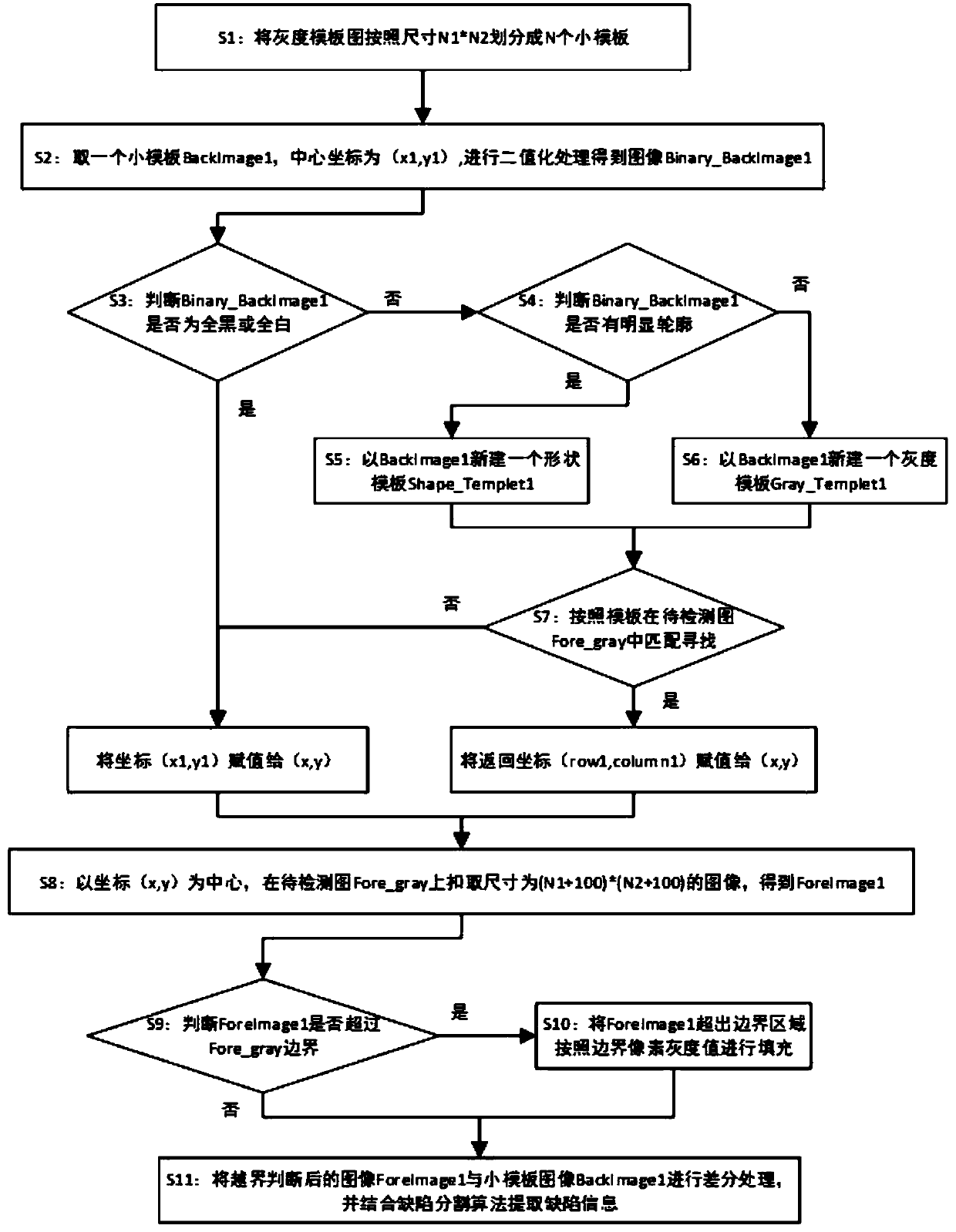
[0020] Embodiment: a PCB board defect location method based on multi-template matching.

[0021] S1, divide the grayscale template image Back_gray into a total of N small templates according to the fixed size N1*N2 (each small template has an overlapping area with the adjacent small template);

[0022] S2, take one of the small template images BackImage1, the center coordinates (x1, y1), and perform binary processing to obtain the image Binary_BackImage1;

[0023] S3, judging whether Binary_BackImage1 is completely black or completely white;

[0024] S4, if it is judged in step S3 that it is all black or all white, assign (x1, y1) to (x, y) if it is not all black or all white, then judge whether there is an obvious outline to Binary_BackImage1;

[0025] S5, if it is judged in step S4 that Binary_BackImage1 has an obvious outline, then create a shape template Shape_Templet1 with BackImage1;

[0026] S6, judging in step S4 that if Binary_BackImage1 has no obvious outline, then...


PUM


Abstract

The invention provides a PCB defect positioning method based on multi-template matching. By dividing a template image and according to the characteristics of divided small template images, relative matching templates are arranged, the error in traditional template matching can be greatly reduced through the PCB defect positioning method, the accumulative error caused by actual image deformation can be further reduced through multi-template matching, border-crossing judgment and automatic pixel filling processing are conducted on a matched area after template matching, and the problem that after border-crossing, the defect detection deviation occurs is also effectively solved through the PCB defect positioning method; and through the PCB defect positioning method, the positioning precisionin the PCB detection early stage can be improved, the accumulative deviation between an actual image and a template image is reduced, the detection efficiency and the detection precision are also effectively improved, and a series of detection requirements for high-precision positioning, matching and the like of the PCB detection process are achieved really.

Description

technical field [0001] The invention relates to the technical field of detection equipment, in particular to a PCB board defect location method based on multi-template matching. Background technique [0002] On-line detection of PCB surface defects is an important part of PCB inspection, which directly affects the accuracy of PCB inspection. With the upgrading of PCB production equipment and production technology, the accuracy and accuracy of PCB defect detection requirements Also getting higher and higher. At present, the traditional machine vision detection algorithms are all based on the feature matching method between the template and the image to be detected. The detection speed of this algorithm is slow, and when the image to be detected is deformed, more interference will be generated, resulting in false detection, and the detection stability is poor. Contents of the invention [0003] Aiming at the deficiencies of the prior art, the present invention provides a PC...

Claims


Application Information

Patent Timeline
Patent Type & Authority Applications(China)
IPC IPC(8): G01N21/88G01N21/956G06T7/00G06T7/73
Inventor 魏登明王华龙张璐张鹏中张美杰
Owner FOSHAN NANHAI GUANGDONG TECH UNIV CNC EQUIP COOP INNOVATION INST
Why Eureka
Try Eureka