Unlock instant, AI-driven research and patent intelligence for your innovation.

A sidewall gate electrode of a nonvolatile 3D NAND memory and its preparation method

A non-volatile, gate electrode technology, applied in the direction of circuits, electrical components, semiconductor devices, etc., can solve problems such as fusing and failure, and achieve the effect of increasing the contact area, ensuring potential balance, and increasing the contact area

Active Publication Date: 2020-11-24
HUAZHONG UNIV OF SCI & TECH
View PDF11 Cites 0 Cited by
  • Summary
  • Abstract
  • Description
  • Claims
  • Application Information

AI Technical Summary

Problems solved by technology

[0005] Aiming at the defects of the prior art, the object of the present invention is to provide a side wall gate electrode of a non-volatile 3D NAND memory and its preparation method, on the basis of ensuring the potential balance of the control gate layer, to solve the problem of increasing the number of stacked layers to After a certain number, the through-connection part that appears after a certain number is subjected to high voltage, and there are device failure problems such as fusing and virtual connection.

Method used


Image

  • A sidewall gate electrode of a nonvolatile 3D NAND memory and its preparation method
  • A sidewall gate electrode of a nonvolatile 3D NAND memory and its preparation method
  • A sidewall gate electrode of a nonvolatile 3D NAND memory and its preparation method

Examples


Embodiment Construction

[0040] In order to make the object, technical solution and advantages of the present invention clearer, the present invention will be further described in detail below in conjunction with the accompanying drawings and embodiments. It should be understood that the specific embodiments described here are only used to explain the present invention, not to limit the present invention.

[0041] The specific steps of the preparation method provided by the embodiments of the present invention are as follows:

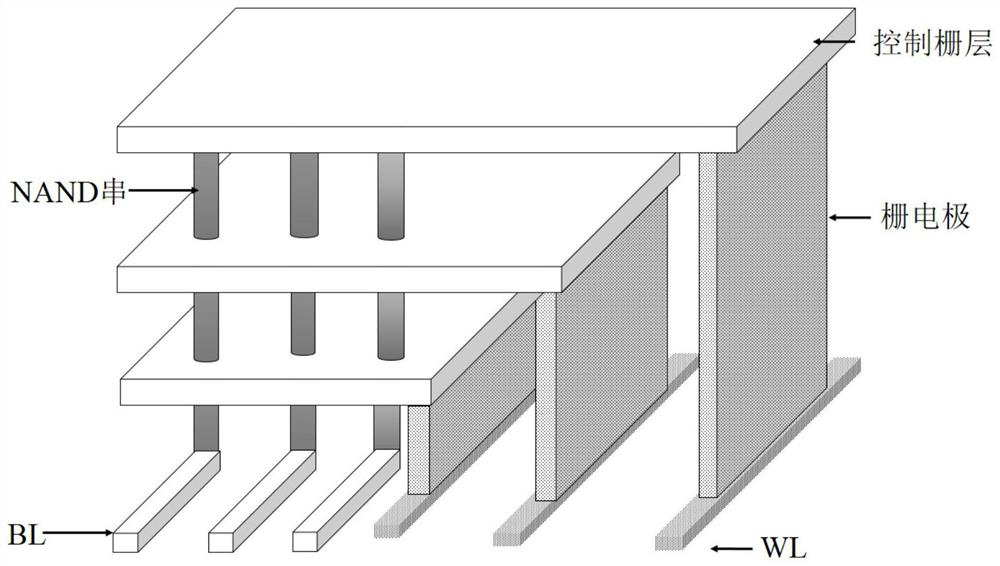
[0042] Such as figure 1, as shown in Figure 2(a) and Figure 2(b), the gate electrode is a spacer-like stepped structure, arranged along the x direction from low to high, and embedded in a multi-layer stacked gate layer and insulating layer. Each gate electrode spacer has upper and lower surfaces, wherein the upper surface of the gate electrode spacer is connected to the corresponding gate layer, and the lower surface is connected to the corresponding word line.

[0043] In th...


PUM

PropertyMeasurementUnit
pore sizeaaaaaaaaaa
widthaaaaaaaaaa

Abstract

The invention discloses a side wall gate electrode of a nonvalatile 3D NAND memory and a manufacturing method thereof. The method comprises the step of manufacturing n gate electrode side wall units which are successively arranged in a stepwise manner through controlling current intensity and an alumina template. Each gate electrode unit is a side wall structure. The upper surface of the side wallgate electrode is used for connecting a gate layer and a lower surface is used for connecting a word line. A side wall gate electrode structure provided in the invention is arranged in the stepwise manner and is connected to different ultra-high stack and corresponding gate layers, and the non-corresponding gate layer in a stack layer and the gate electrode are isolated through an insulating layer. The electrode and the method are suitable for solving a problem that the ultra-high-stack nonvalatile 3D NAND memory repeatedly applies a high voltage so as to cause the fusing of a control gate layer and the gate electrode, virtual connection and other device failure problems.

Description

technical field [0001] The invention belongs to the technical field of microelectronic devices, and more specifically relates to a sidewall gate electrode of a nonvolatile 3D NAND memory and a preparation method thereof. Background technique [0002] In order to meet the development of high-efficiency and low-cost microelectronics industry, semiconductor memories need to have higher integration density. High density is critical to reducing the cost of semiconductor products. For traditional two-dimensional and planar semiconductor memories, their integration density mainly depends on the unit area occupied by a single storage device, and the integration degree is very dependent on the quality of the mask process. However, even if expensive process equipment is continuously used to improve the mask process precision, the increase in integration density is still very limited. Especially with the development of Moore's Law, below the 22nm process node, planar semiconductor me...

Claims


Application Information

Patent Timeline
Patent Type & Authority Patents(China)
IPC IPC(8): H01L21/28H01L27/11524H01L27/1157
Inventor 缪向水杨哲童浩
Owner HUAZHONG UNIV OF SCI & TECH