
Method and equipment for chemical mechanical planarization

A chemical-mechanical, planarization technology, applied in metal processing equipment, grinding/polishing equipment, grinding machine tools, etc., to solve the problems of wafer flatness and thickness uniformity that are difficult to maintain

Active Publication Date: 2021-05-28
TAIWAN SEMICON MFG CO LTD
View PDF9 Cites 0 Cited by
  • Summary
  • Abstract
  • Description
  • Claims
  • Application Information

AI Technical Summary

Problems solved by technology

Flatness and thickness uniformity across the wafer becomes more difficult to maintain in this larger wafer

Method used


Image

  • Method and equipment for chemical mechanical planarization
  • Method and equipment for chemical mechanical planarization
  • Method and equipment for chemical mechanical planarization

Examples


Embodiment Construction

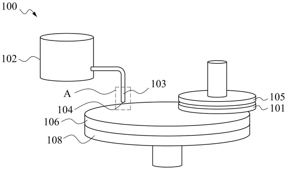
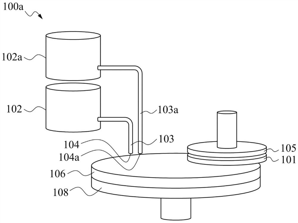
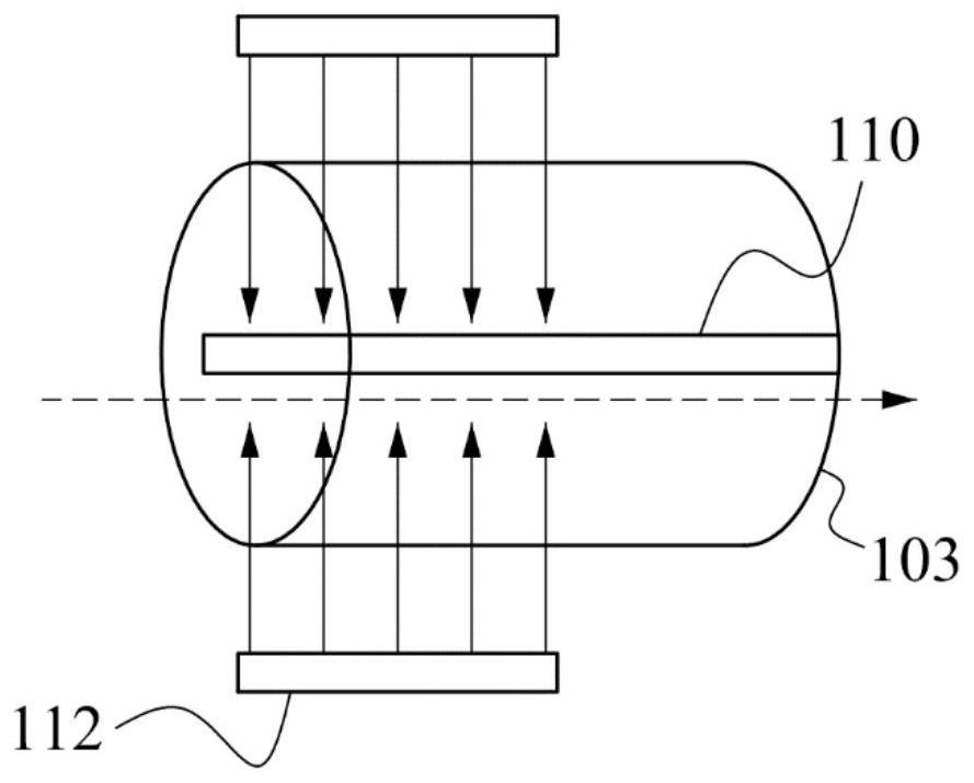
[0021] The following disclosure provides many different embodiments, or illustrations, for implementing different features of the invention. Specific illustrations of components and arrangements are described below to simplify the present disclosure. These are of course only examples and are not intended to be limiting. For example, the description that the first feature is formed on or above the second feature includes the embodiment that the first feature and the second feature are in direct contact, and also includes that other features are formed between the first feature and the second feature, An embodiment such that the first feature and the second feature are not in direct contact. The dimensions of many features may be drawn at different scales for simplicity and clarity. In addition, the present disclosure repeats element symbols and / or letters in various illustrations. This repetition is for simplicity and clarity and does not imply any relationship between the v...


PUM

PropertyMeasurementUnit
thicknessaaaaaaaaaa
wavelengthaaaaaaaaaa
strengthaaaaaaaaaa

Abstract

The present disclosure provides a chemical mechanical planarization method and equipment thereof, in particular a chemical mechanical planarization equipment and a method for connecting semiconductor substrates using the chemical mechanical planarization equipment. According to some embodiments, an apparatus includes: a pad disposed on a rotatable platform; a carrier head disposed on the pad, and the carrier head is configured to hold a semiconductor substrate between the pad and the carrier head; configured to accommodate A tank containing a liquid containing a composition; at least one tube fluidly coupled to the tank, and the at least one tube includes a photocatalyst; a nozzle fluidly coupled to the tank through the at least one tube, and the nozzle is configured to provide the liquid containing the composition to the pad; and a light source configured to provide light to irradiate the photocatalyst and the liquid containing the composition flowing through at least one pipe.

Description

technical field [0001] The present disclosure relates to a method for manufacturing a semiconductor device, in particular to a method for performing chemical mechanical planarization and related equipment. Background technique [0002] The present disclosure relates to a method of manufacturing a semiconductor device. In particular, the disclosed subject matter relates to a method for performing chemical mechanical polishing (CMP) and related equipment. [0003] Chemical mechanical polishing / planarization (CMP) is an important process for smoothing the surface of a semiconductor wafer, which smoothes the surface of the semiconductor wafer by both chemical etching and physical polishing. The semiconductor wafer is mounted on a polishing head, wherein the polishing head is rotated in a chemical mechanical polishing process. The rotating grinding head is pressed against the semiconductor wafer against the rotating grinding pad. A polishing solution containing chemical etchan...

Claims


Application Information

Patent Timeline
Patent Type & Authority Patents(China)
IPC IPC(8): B24B37/00B24B37/34
CPCH01L21/02024H01L22/20H01L22/12B24B57/02B24B37/105H01L21/31055H01L21/6715H01L21/67092H01L21/67075B24B37/00
Inventor 刘文贵
Owner TAIWAN SEMICON MFG CO LTD
Learn More