

Circuit board defect detection method and device
A defect detection and circuit board technology, used in character and pattern recognition, image data processing, instruments, etc., can solve the problems of high detection cost, low efficiency and low accuracy, and achieve the effect of improving accuracy and efficiency
- Summary
- Abstract
- Description
- Claims
- Application Information
AI Technical Summary
Problems solved by technology
Method used
Image

Examples
Embodiment Construction
[0051]Embodiments of the present application are described in detail below, examples of which are shown in the drawings, wherein the same or similar reference numerals denote the same or similar elements or elements having the same or similar functions throughout. The embodiments described below by referring to the figures are exemplary, and are intended to explain the present application, and should not be construed as limiting the present application.
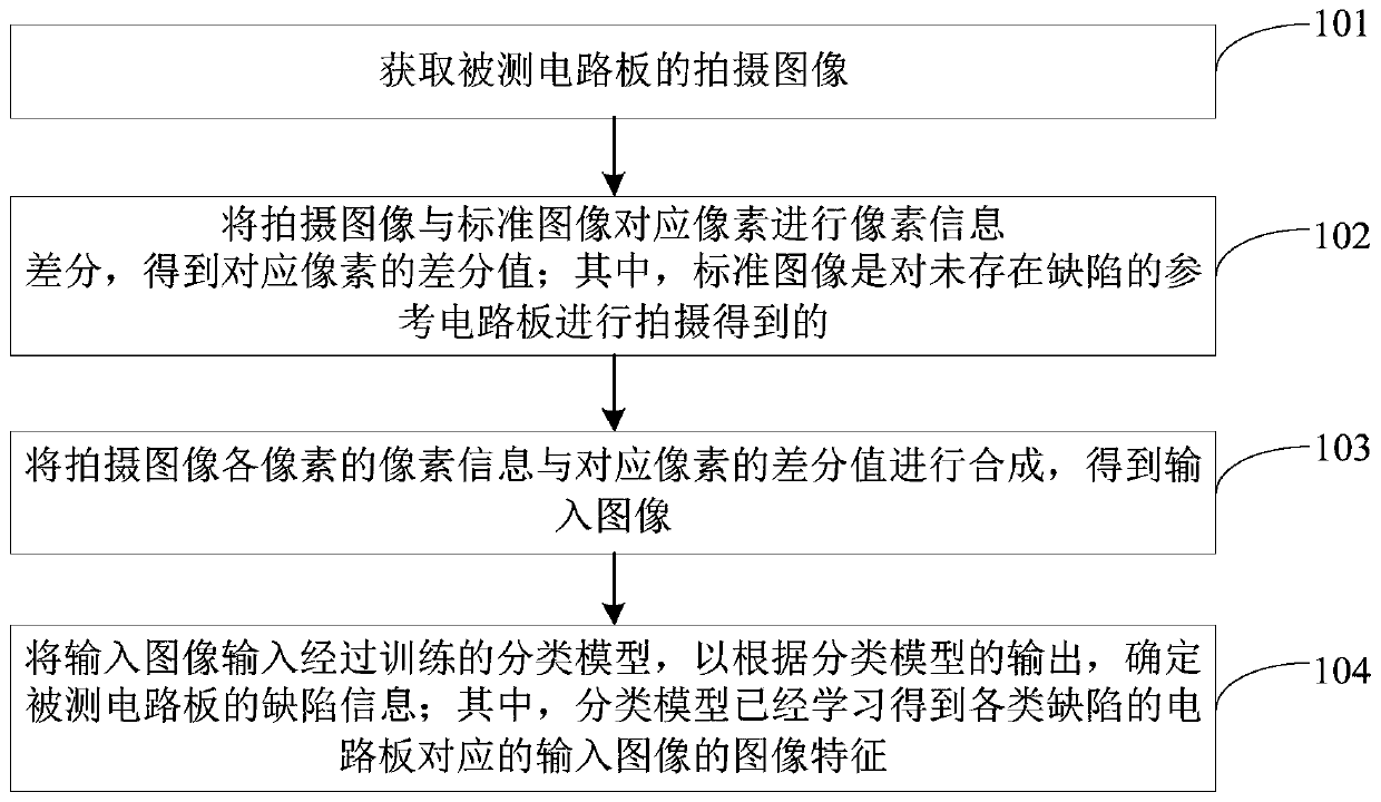
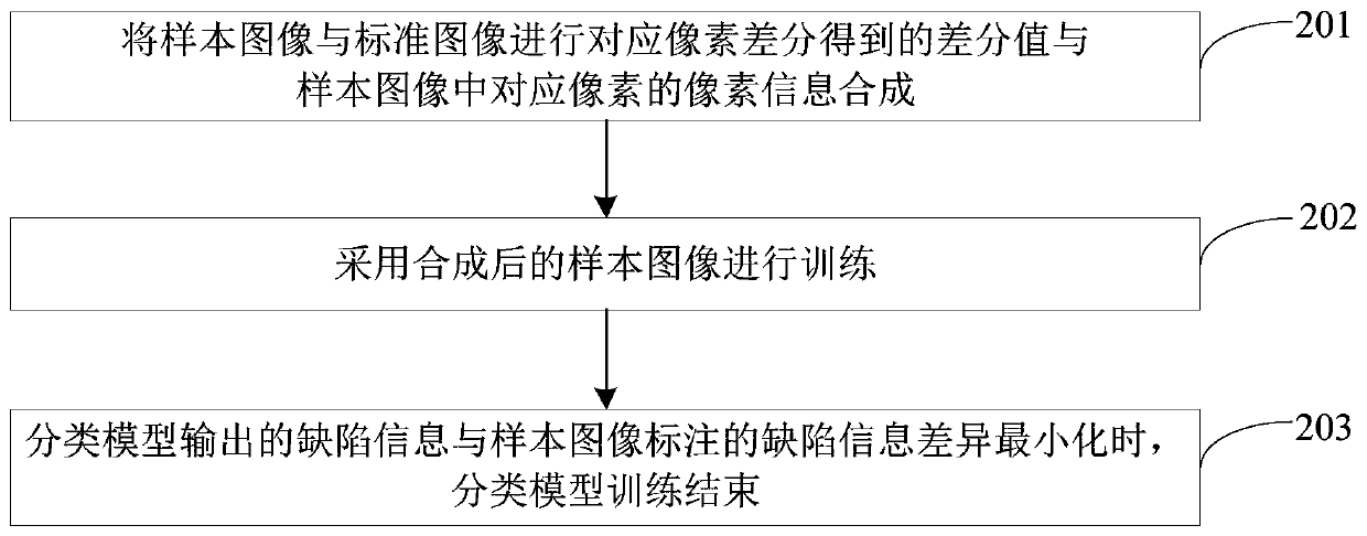
[0052] The embodiment of this application aims at the technical problems of high detection cost, low accuracy of detection results and poor real-time performance in the prior art where the detection of circuit board defects relies on purely manual detection methods, and proposes a circuit board defect detection method.
[0053] The circuit board defect detection method provided by the embodiment of the present application obtains the photographed image of the circuit board under test, and performs pixel information difference...
PUM
 Abstract
Description
Claims
Application Information