Method and circuit for testing multi-clock domain

A technology with multiple clock domains and test methods, applied in the direction of measuring electricity, measuring electrical variables, electronic circuit testing, etc. The effect of testing efficiency

Active Publication Date: 2011-09-14
HISENSE VISUAL TECH CO LTD
View PDF5 Cites 15 Cited by
  • Summary
  • Abstract
  • Description
  • Claims
  • Application Information

AI Technical Summary

Problems solved by technology

[0005] The present invention aims at the shortcomings of the prior art that different clock domains cannot be uniformly controlled when testing integrated chips, and circuits across multiple clock domains cannot

Method used


Image

  • Method and circuit for testing multi-clock domain
  • Method and circuit for testing multi-clock domain
  • Method and circuit for testing multi-clock domain

Examples


Example Embodiment

[0034] The technical solutions of the present invention will be further described in detail below in conjunction with the accompanying drawings and specific embodiments.

[0035] The present invention considers that when testing a chip in the prior art, due to the existence of multiple clock domains, each clock domain needs to be tested separately, and there are problems such as complicated testing process and inability to correctly test cross-clock domain circuits, etc., and proposes a A multi-clock domain testing method, the core idea of ​​this method is to set the clock domain selection signal, and use this signal to control one or more clock domains as clock domains that can be tested. In this way, not only can multiple clock domains work simultaneously, In order to improve the test efficiency, and can eliminate the mutual influence between different clock domains, and solve the problem of cross-clock domain circuit testing.

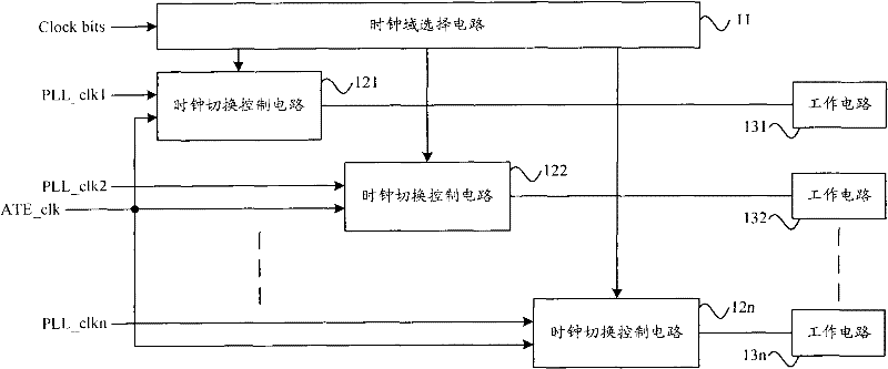
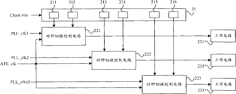
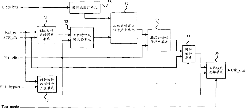
[0036] figure 1 Shown is a structural block d...


PUM


Abstract

The invention discloses a method and a circuit for testing a multi-clock domain. The multi-clock domain comprises a plurality of working clocks. The method for testing the multi-clock domain comprises the following steps that: each working clock and each testing clock in each clock domain provide a corresponding clock for a working circuit through a clock switching control circuit; a selection signal of each clock domain is set to provide a working enable signal for the clock switching control circuit in each clock domain; the effectiveness or ineffectiveness of the working enabling of different clock switching control circuits is controlled by the selection signal of each clock domain; and a test state of the clock domain corresponding to the clock switching control circuit is controlled. By the method and the circuit for testing the multi-clock domain, simultaneous test on circuits in the multi-clock domain and test on circuits in a cross-clock domain simultaneously are realized.

Description

technical field [0001] The invention belongs to the technical field of testing integrated chips, and in particular relates to a multi-clock domain testing method and a testing circuit when testing chips. Background technique [0002] In the process of designing and generating integrated chips used in digital TVs and set-top boxes, it is often necessary to add DFT design (design for testability) in order to test whether there are problems such as short circuit and open circuit in the chip manufacturing. Usually, a specific test clock is required for chip testing, which is called an ATE clock; and a clock that the chip works normally is called an operating clock. Generally speaking, the frequency of the ATE clock is usually lower than the normal working clock of the chip in practical applications. Therefore, in order to ensure the accuracy of the test, the working clock of the chip is usually used as the capture clock for capturing data. Therefore, when the chip is tested, th...

Claims


Application Information

Patent Timeline
IPC IPC(8): G01R31/28G01R31/02H03K5/13H03K5/135H03K5/14
Inventor 邱敏
Owner HISENSE VISUAL TECH CO LTD
Why Eureka
Try Eureka