Electronic device, shell assembly and processing method thereof
A technology of shell assembly and processing method, which is applied in the direction of cabinet/cabinet/drawer parts, decorative art, decorative structure, etc., can solve the problems of decreased anti-drop performance, easy cracking of plate structure, and inability to meet user needs. , to achieve the effect of strong structural strength and improved anti-drop characteristics
- Summary
- Abstract
- Description
- Claims
- Application Information
AI Technical Summary
Problems solved by technology
Method used
Image

Examples
Embodiment 1
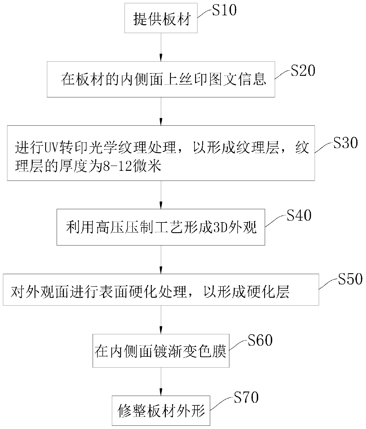
[0044] Such as figure 1 , figure 2 As shown, the processing method of the shell assembly 100 includes the following steps:
[0045] S10: Provide a sheet material 101, which includes an opposite appearance surface and an inner surface. It should be noted that the board is a flat composite board.
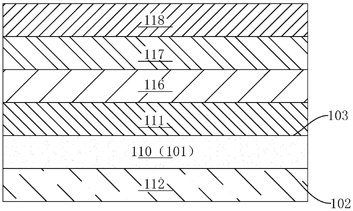
[0046] S20: Silk-screen graphic information (such as LOGO) on the inner surface of the board 101 . It should be noted that when the plate 101 is processed, multiple layered structures can be constructed, such as the texture layer 111 and the hardened layer 112. These layered structures can protect the graphic information formed by silk screen printing, thereby It can prevent the graphic information from being worn out. For example, the panel 101 may be a 2.5D composite panel or a planar composite panel.
[0047] S30: Perform UV transfer optical texture treatment on the inner surface of the plate 101 to form a texture layer 111, the thickness of the texture layer 111 is 8um-12um....
Embodiment 2
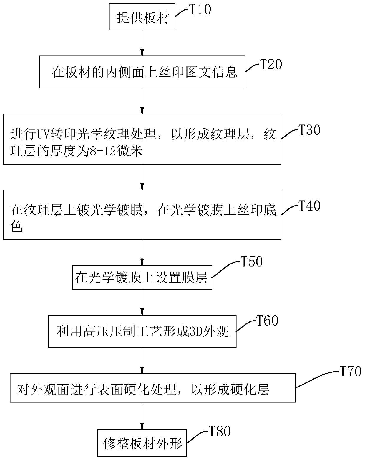
[0055] Such as image 3 , Figure 4 As shown, the processing method of the shell assembly 100 includes the following steps:
[0056] T10: Provide a board 101, the board 101 includes opposite exterior surfaces and inner surfaces. It should be noted that the board 101 can be a board-shaped material with a certain curvature, three-dimensional effect, or planar effect, and it can be a board 101 composed of multiple materials.
[0057] T20: Silk-screen graphic information (such as LOGO) on the inner surface of the board 101 . It should be noted that when the plate 101 is processed, multiple layered structures can be constructed, such as the texture layer 111 and the hardened layer 112. These layered structures can protect the graphic information formed by silk screen printing, thereby It can prevent the graphic information from being worn out. In some embodiments, the sheet 101 may be a 2.5D composite sheet or a planar composite sheet.
[0058] T30: Perform UV transfer optical...
PUM
| Property | Measurement | Unit |
|---|---|---|
| Thickness | aaaaa | aaaaa |
| Thickness | aaaaa | aaaaa |
| Thickness | aaaaa | aaaaa |
Abstract
Description
Claims
Application Information