Tile for an active electronically scanned array (AESA)

A technology of electronic scanning and tiling, applied in antenna arrays, modular arrays, specific array feeding systems, etc., can solve problems such as inoperability of active circuits

Active Publication Date: 2019-06-14
RAYTHEON CO
View PDF6 Cites 4 Cited by
  • Summary
  • Abstract
  • Description
  • Claims
  • Application Information

AI Technical Summary

Problems solved by technology

Excessive heat can render

Method used


Image

  • Tile for an active electronically scanned array (AESA)
  • Tile for an active electronically scanned array (AESA)
  • Tile for an active electronically scanned array (AESA)

Examples


Embodiment Construction

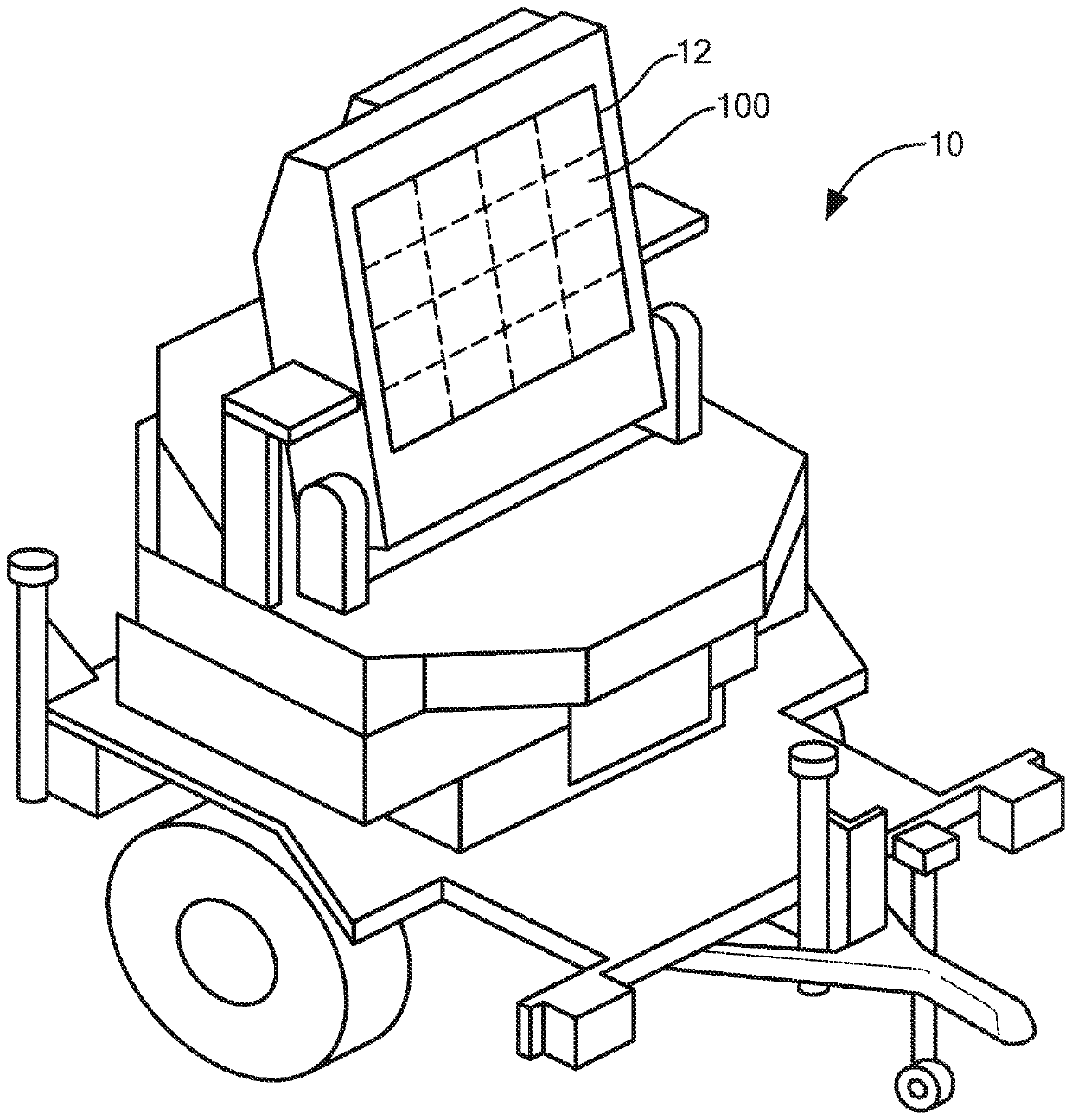
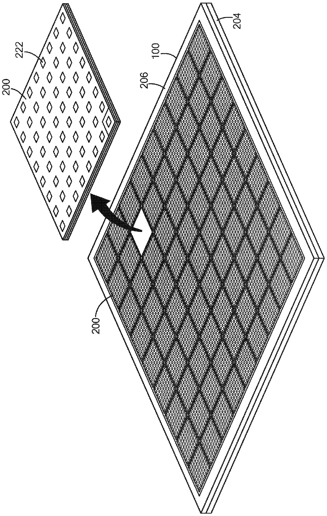
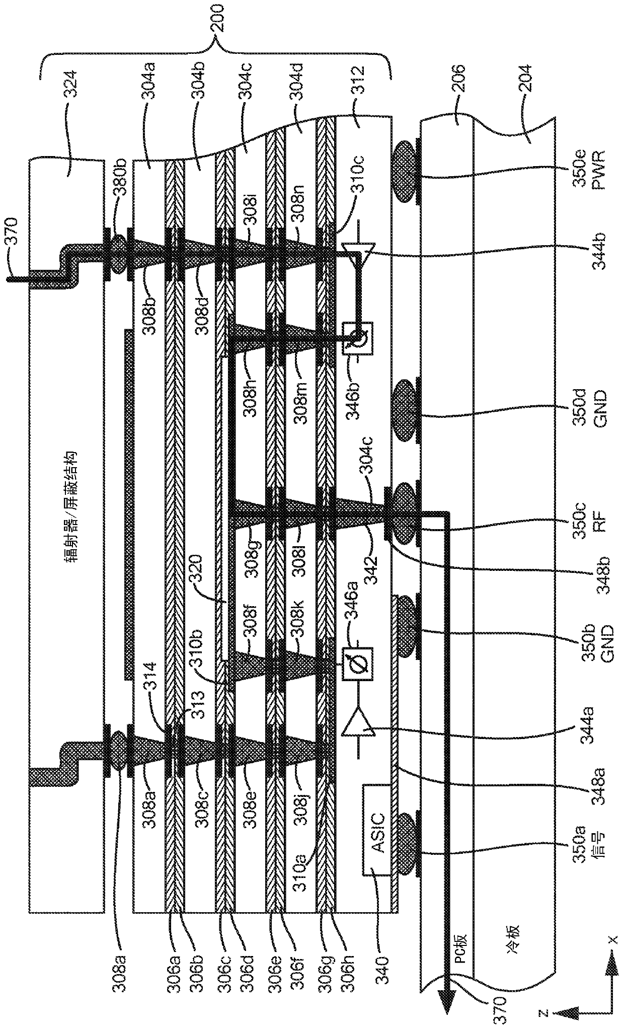
[0011] Described herein are millimeter-wave radio frequency (RF) tiles that function as active electronically scanned arrays (AESAs) and are scalable to form, for example, larger NxN AESAs. As described herein, the tiles incorporate low-loss glass RF manifolds that are wafer-level bonded directly to beamforming circuits and radiation shielding radiators.

[0012] As understood in the art, higher frequencies require tighter lattice spacing between active elements, which leaves less room for active circuitry. This becomes even tighter when λ / 2 (half wavelength at the emission frequency) spacing is required for wide scan angles. The tile structure described herein enables signals to pass through the Z-axis, for example using vias, allowing higher frequencies such as Ka-band and beyond. One or more tiles can be mounted to a printed circuit board, which enables scalability. For example, tiles provide high-density RF packaging and interconnects. In one example, the tiles include ...


PUM


Abstract

In one aspect, an active electronically scanned array (AESA) tile includes a radiator structure and oxide-bonded semiconductor wafers attached to the radiator structure and comprising a radio frequency (RF) manifold and a beam former. An RF signal path through the oxide-bonded wafers comprises a first portion that propagates toward the beam former and a second portion that propagates parallel to the beam former.

Description

Background technique [0001] As is known in the art, a phased array antenna includes a plurality of active circuits spaced apart from each other by a known distance. Each active circuit is coupled to either or both the transmitter and receiver through a plurality of phase shifter circuits, amplifier circuits, and / or other circuits. In some cases, phase shifters, amplifier circuits, and other circuits (e.g., mixer circuits) are provided in so-called transmit / receive (T / R) modules and are considered part of the transmitter and / or receiver . [0002] Phase shifters, amplifiers, and other circuits (eg, T / R modules) often require external power sources (eg, DC power supplies) to operate properly. Therefore, these circuits are referred to as "active circuits" or "active components". Therefore, phased array antennas that include active circuitry are often referred to as "active phased arrays." Active phased array radar is also known as an active electronically scanned array (AESA)...

Claims


Application Information

Patent Timeline
IPC IPC(8): H01Q21/00H01Q23/00
CPCH01Q23/00H01Q21/061H01Q1/02H01Q21/0075H01Q3/36H01Q1/526H01Q21/0025H01L25/0655H01L23/66H01L23/552H01L2224/16227H01L24/08H01L24/05H01L2224/94H01L24/94H01L2224/13025H01L2224/05025H01L2224/80896H01L2224/80902H01L24/02H01L2224/13024H01L2224/05647H01L2224/05655H01L2224/05624H01L2224/05008H01L2224/02372H01L2224/04H01L2224/08146H01L24/13H01L24/16H01L24/06H01L2224/06181H01L24/80H01L24/73H01L2224/73251H01L2924/1421H01L2224/05686H01L2224/05576H01L2224/131H01L2224/80H01L2924/00014H01L2924/05442H01L2224/08H01L2224/16H01L2924/014H01L23/367H01L24/29H01L24/32H01L25/18H01L2223/6672H01L2223/6677H01L2223/6627H01L2223/6622
Inventor M·A·手柴J·G·米尔恩K·C·罗尔斯顿J·J·德拉布
Owner RAYTHEON CO
Why Eureka
Try Eureka