

Wearable device
A wearable device and chip technology, applied in the direction of electrical components, circuits, printed circuits, etc., can solve the problem of low utilization rate of circuit boards
- Summary
- Abstract
- Description
- Claims
- Application Information
AI Technical Summary
Problems solved by technology
Method used
Image


Examples
Embodiment 1
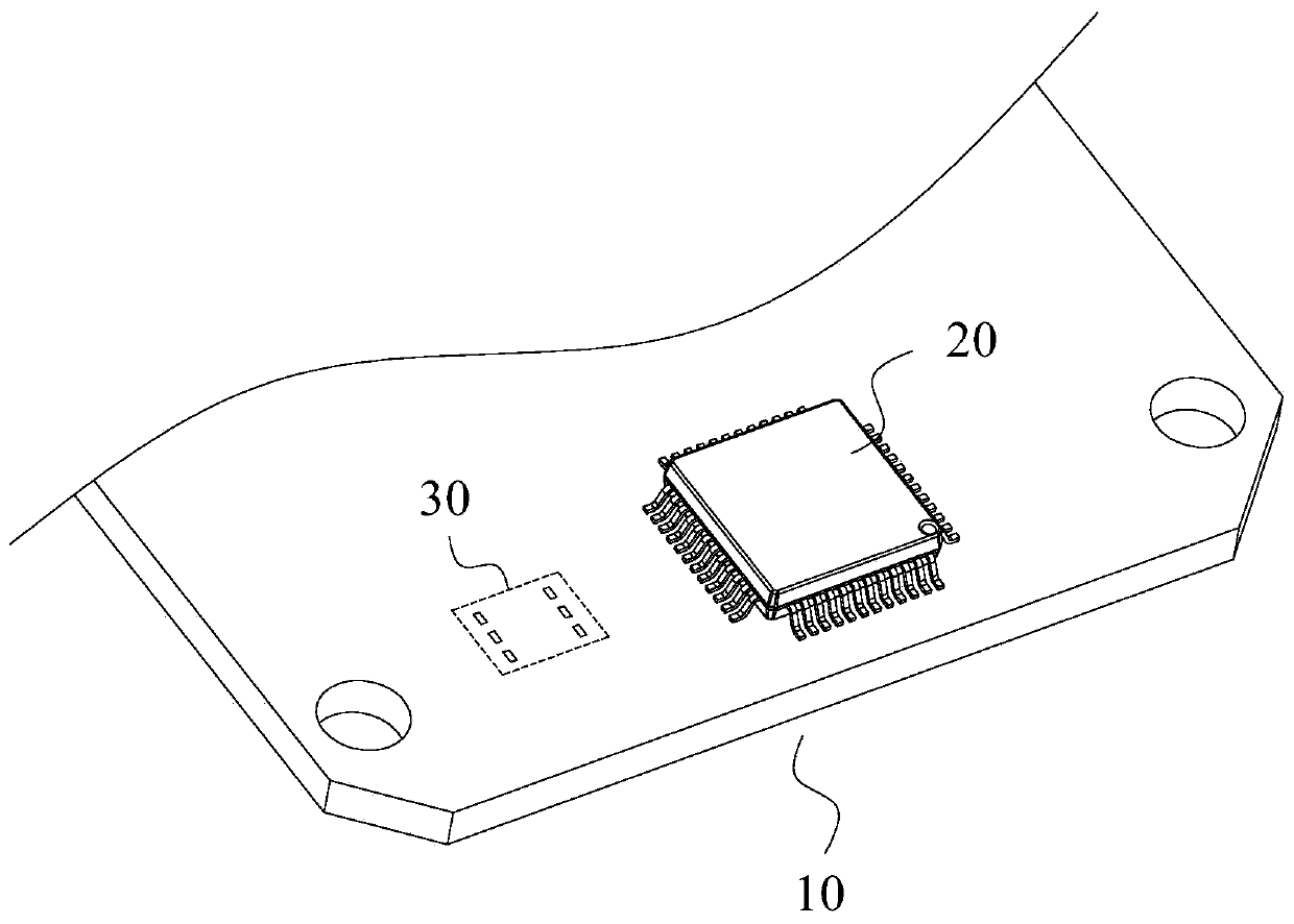
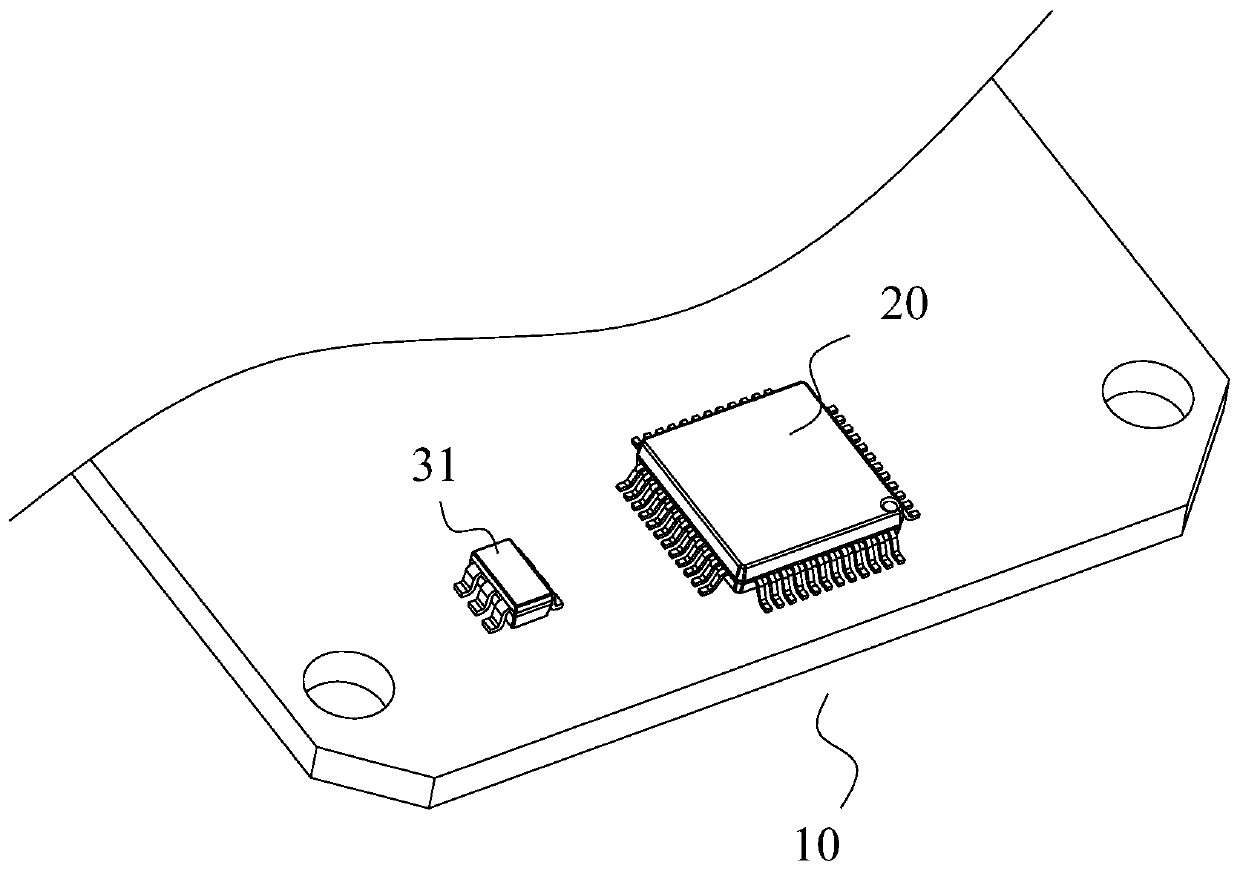
[0025] figure 1 and figure 2 They are the first internal structure and the second internal structure diagram of a wearable device provided in Embodiment 1 of the present application. This embodiment is applicable to various wearable devices, such as smart glasses and smart watches. The device specifically includes a main circuit board 10 and a main controller 20, and also includes a first chip or a second chip, and the first chip and the second chip are chips with different functions;
[0026] The main circuit board 10 is provided with a general-purpose pad group 30, at least one pad in the general-purpose pad group 30 is defined as a signal input pad, and at least one pad in the general-purpose pad group 30 is defined as a signal input pad. An output pad, at least one pad in the general-purpose pad group 30 is defined as a ground pad;
[0027] The first chip and the second chip include signal input pins, signal output pins and ground pins, and the pin layout after packagin...
PUM
 Abstract
Description
Claims
Application Information