
Algorithm for reducing write-in amplification rate and improving random write-in performance

A random write and magnification technology, applied in computing, instruments, electrical and digital data processing, etc., to slow down FLASH life loss, improve random write speed, and reduce write magnification.

Pending Publication Date: 2019-07-26
SHENZHEN SHICHUANGYI ELECTRONICS
View PDF15 Cites 3 Cited by
  • Summary
  • Abstract
  • Description
  • Claims
  • Application Information

AI Technical Summary

Problems solved by technology

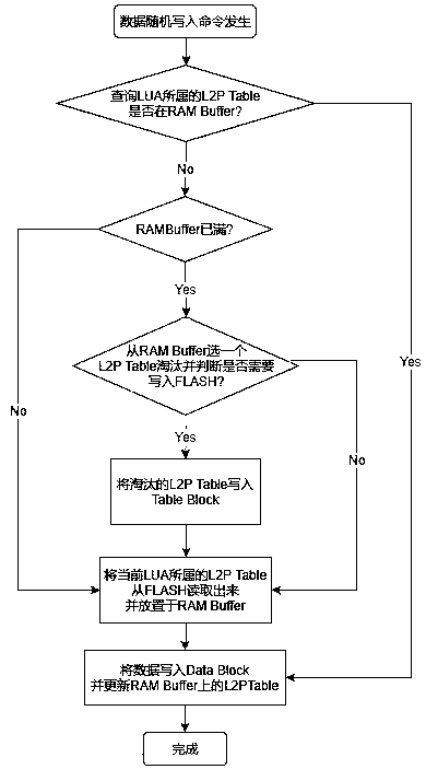
The size of each L2P Table is 16K bytes, so FLASH needs to prepare a total of 32M bytes of space for storage, but when the RAMbuffer of the main control chip cannot prepare the same 32M bytes of space to load 2048 L2P Tables, L2P Table replacement will occur , while the RAM buffer provided by the general master chip is far less than 32MB bytes

Method used


Image

  • Algorithm for reducing write-in amplification rate and improving random write-in performance
  • Algorithm for reducing write-in amplification rate and improving random write-in performance

Examples


Embodiment Construction

[0021] The preferred embodiments of the present invention will be described in detail below in conjunction with the accompanying drawings, so that the advantages and features of the invention can be more easily understood by those skilled in the art, so as to define the protection scope of the present invention more clearly.

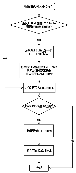
[0022] Such as figure 2 As shown, it is a flow chart of the algorithm for reducing write amplification and improving random write performance of the present invention, including the following steps:

[0023] Step 1, a logical address LBA data random write command occurs;

[0024] Step 2. Query whether the L2P Table to which the LUA belongs is in the RAM Buffer. If it is not in step 3, if it is in step 5;

[0025] Step 3. Select an L2P Table from the RAM Buffer to eliminate;

[0026] Step 4, read from the FLASH from the L2P Table to which the current LUA belongs and place it in the RAM Buffer;

[0027] Step 5. Write data into DateBlock;

[0028] Step...


PUM


Abstract

The invention discloses an algorithm for reducing the write-in amplification rate and improving the random write-in performance. The method and the device are suitable for a storage device product carrying a flash memory; the key point of the algorithm of the invention is to update L2P Tablets in batches; the method comprises the following steps: a write-in data volume is determined; the algorithmis defined as a data block (Data Block), before the Data Block is not fully written, after data are written in, the L2P Table on the RAM Buffer does not need to be immediately updated, batch updatingis carried out after the Data Block is fully written in, and in the batch updating process, code variables are used as a bit table to carry out grouping on updated and unupdated entity addresses, sothat the number of times of code cyclic operation is reduced. According to the algorithm provided by the invention, the code cycle operation frequency and the FLASH write-in frequency are reduced, therandom write-in speed is greatly improved, and the write-in amplification rate is reduced, so that the FLASH life loss is reduced.

Description

technical field [0001] The invention relates to the technical field of storage equipped with FLASH memory, in particular to an algorithm for reducing write amplification and improving random write performance. Background technique [0002] In the digital storage solution equipped with FLASH memory, the FLASH translation layer (FLASH TRANSLATIONLAYER, referred to as FTL) algorithm is a key factor in product performance and life. The FTL algorithm includes many complex and exploratory modules. Among them, the logic-to-physical address mapping table Control is one of the most important links. [0003] The current FTL algorithm is as follows: when a logical address is randomly written, FTL needs to prepare the FLASH space for the data of this logical address for storage, and the logical address data is actually written to which physical address of the FLASH, it needs a logical to Physical address mapping table (Logical address to Physical address Table, referred to as L2PTable)...

Claims


Application Information

Patent Timeline
Patent Type & Authority Applications(China)
IPC IPC(8): G06F12/06G06F12/123
CPCG06F12/0646G06F12/123G06F12/0623
Inventor 倪黄忠
Owner SHENZHEN SHICHUANGYI ELECTRONICS
Learn More