Wafer transport carrier and wafer box detection method

A wafer box and wafer technology, applied in the direction of transportation and packaging, conveyor objects, electrical components, etc., can solve unsatisfied problems, achieve the effect of reducing wafer scrapping and preventing the door panel from falling off the shell

Active Publication Date: 2019-07-26
TAIWAN SEMICON MFG CO LTD
View PDF11 Cites 2 Cited by
  • Summary
  • Abstract
  • Description
  • Claims
  • Application Information

AI Technical Summary

Problems solved by technology

While current overhead handling systems are fit for purpose, they have not met many other requirements

Method used


Image

  • Wafer transport carrier and wafer box detection method
  • Wafer transport carrier and wafer box detection method
  • Wafer transport carrier and wafer box detection method

Examples


Embodiment Construction

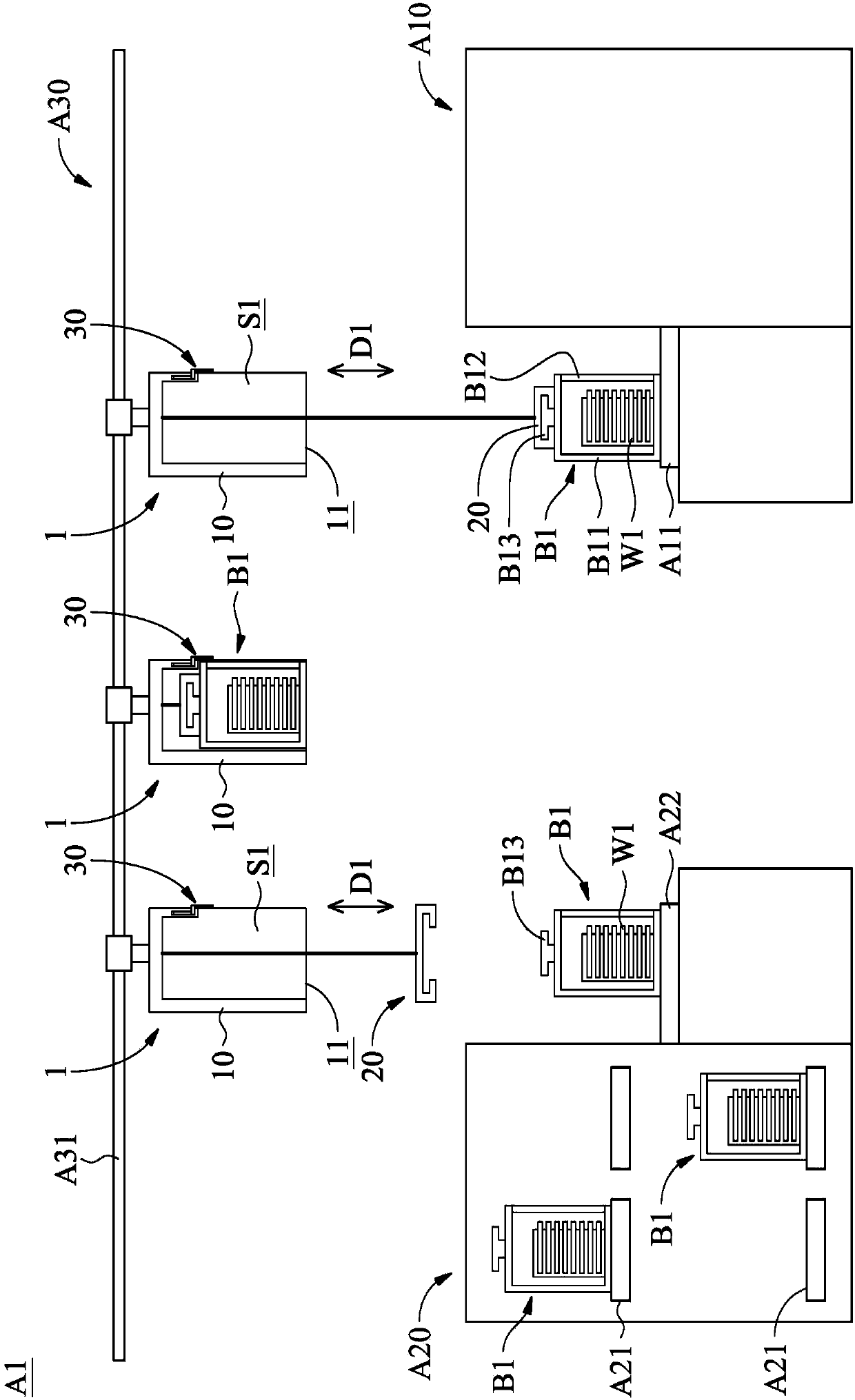
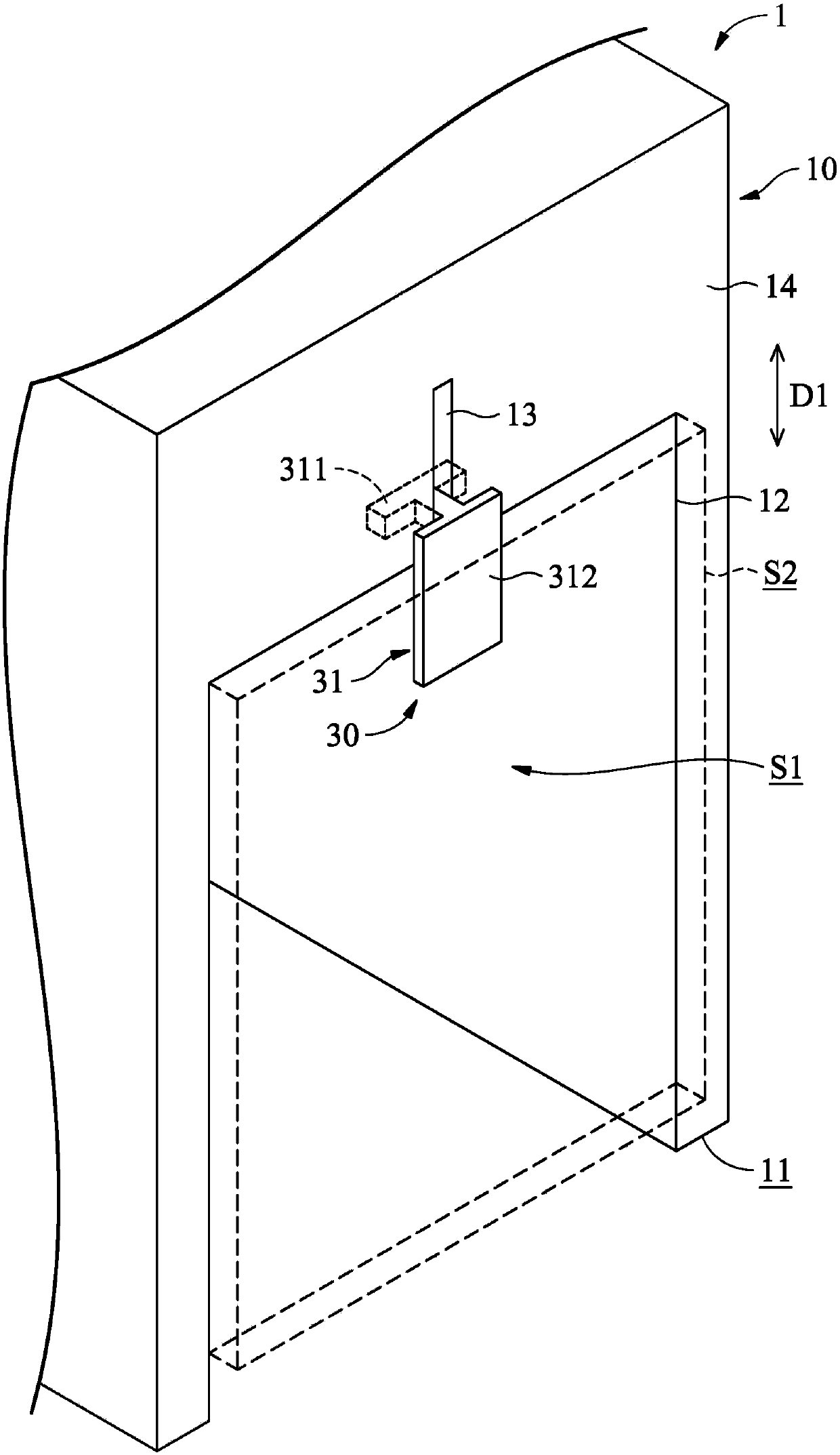
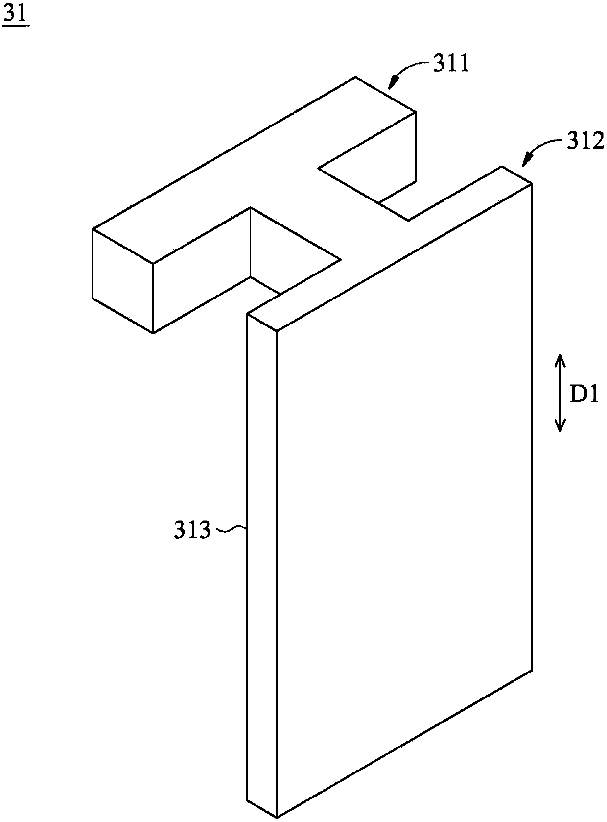
[0053] The following description provides many different embodiments, or examples, for implementing various features of the disclosure. The elements and arrangements described in the following specific examples are only used to briefly express the embodiments of the present disclosure, which are only examples and not intended to limit the embodiments of the present disclosure. For example, a description of a first feature on or over a second feature includes direct contact between the first and second features, or another feature disposed between the first and second features such that the second feature The first and second features are not in direct contact.

[0054] In addition, in this specification, the same reference numerals and / or words are used in different examples. The aforementioned repetition is only for simplification and clarity, and does not mean that different embodiments and settings must be related.

[0055] Words such as first and second in this specifica...


PUM


Abstract

The invention provides a wafer transport carrier and a wafer box detection method. The wafer transport carrier comprises a loading device with a containing space and a detection area which is connected with the containing space, a suspension device arranged in the containing space and configured to move a wafer box into the containing space, and a detection device arranged on the loading device and configured to detect the position of a door plate of the wafer box so as to send out a warning signal when the door plate is located in the detection area. The detection device disclosed by the invention can be used for detecting whether the door plate of the wafer box is loosened relative to a shell or not in real time in a process that the suspension device moves the wafer box or in a processthat the wafer transport carrier transports the wafer box, and can be used for sending out the warning signal when detecting that the door plate is loosened relative to the shell, so that the door plate can be prevented from falling from the shell and the risk of wafer scrap can be reduced.

Description

technical field [0001] The present disclosure mainly relates to a wafer transport carrier and a detection method for a wafer box, and particularly relates to a wafer transport carrier with a detection device and a detection method for detecting a wafer cassette by using the detection device. Background technique [0002] Semiconductor devices have been used in various electronic applications, such as personal computers, cell phones, digital cameras, and other electronic devices. Semiconductor devices are basically sequentially deposited by depositing insulating or dielectric layers, conductive layers, and semiconductor layer materials onto a wafer, and using lithography to pattern the various material layers to form circuit components and components thereon manufacture. Many integrated circuits are generally fabricated on a single wafer, and individual dies on the wafer are diced and separated between the integrated circuits along a dicing line. For example, individual die...

Claims


Application Information

Patent Timeline
Patent Type & Authority Applications(China)
IPC IPC(8): H01L21/67H01L21/677
CPCH01L21/67733H01L21/67253
Inventor 詹翔安李忠宪萧凤儒
Owner TAIWAN SEMICON MFG CO LTD
Why Eureka
Try Eureka