Optical component, manufacturing method thereof, bonding method, and display device

A technology for optical components and optical adhesive layers, which can be used in bonding methods, chemical instruments and methods, identification devices, etc., and can solve problems such as low bonding accuracy

Active Publication Date: 2021-10-01
BOE TECH GRP CO LTD +1
View PDF0 Cites 0 Cited by
  • Summary
  • Abstract
  • Description
  • Claims
  • Application Information

AI Technical Summary

Problems solved by technology

[0004] The present invention at least partly solves the problem of low bonding precision when the existing optical glue is applied to the bonding process of display device manufacturing, and provides an optical component, a manufacturing method of an optical component, a bonding method, and a display device. device

Method used


Image

  • Optical component, manufacturing method thereof, bonding method, and display device
  • Optical component, manufacturing method thereof, bonding method, and display device
  • Optical component, manufacturing method thereof, bonding method, and display device

Examples


Embodiment 1

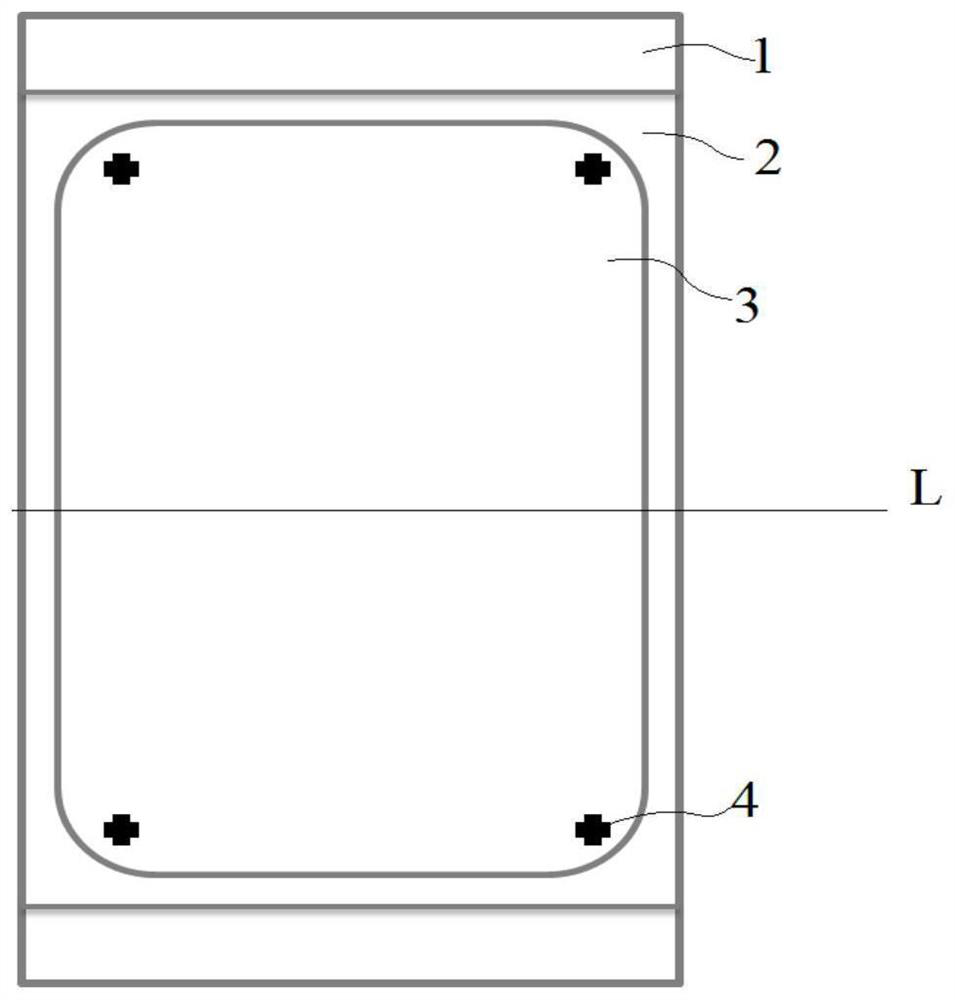
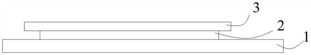
[0021] combine figure 1 and figure 2 , the present embodiment provides an optical assembly, including a stacked first release film 1, an optical adhesive layer 2, and a second release film 3, on the surface of the optical adhesive layer 2 facing away from the first release film 1 At least one alignment mark 4 is also provided, and the material of the alignment mark 4 includes an up-conversion luminescent material, which can convert infrared light into visible light.

[0022] If the first release film 1 is a heavy release film, the second release film 3 is a light release film. If the first release film 1 is a light release film, the second release film 3 is a heavy release film. In the above solution, the alignment mark 4 is made on the optical adhesive layer 2, or it is made on the heavy release film as in the prior art. Of course, the alignment mark 4 can be made on the surface of the optical adhesive layer 2 facing the heavy release film, or on the surface of the optica...

Embodiment 2

[0030] combine figure 1 and figure 2 , this embodiment provides a method for manufacturing an optical component, including the following steps.

[0031] In step S1, an optical adhesive layer 2 attached with a first release film 1 is provided.

[0032] In step S2, at least one alignment mark 4 is formed on the surface of the optical adhesive layer 2 facing away from the first release film 1, the material of the alignment mark 4 includes an up-conversion luminescent material, and the up-conversion luminescent material can convert infrared light for visible light.

[0033] Of course, an up-conversion luminescent material needs to be prepared. The above conversion luminescent material is NaGdF4:Er3 + Nanoparticles are taken as an example.

[0034] First, the Er(NO 3 ) 3 , Yb(NO 3 ) 3 and Gd(NO 3 ) 3 (The above three are usually in powder form or dissolved in solution) into deionized water, and at the same time add ethylenediaminetetraacetic acid (EDTA, usually in powde...

Embodiment 3

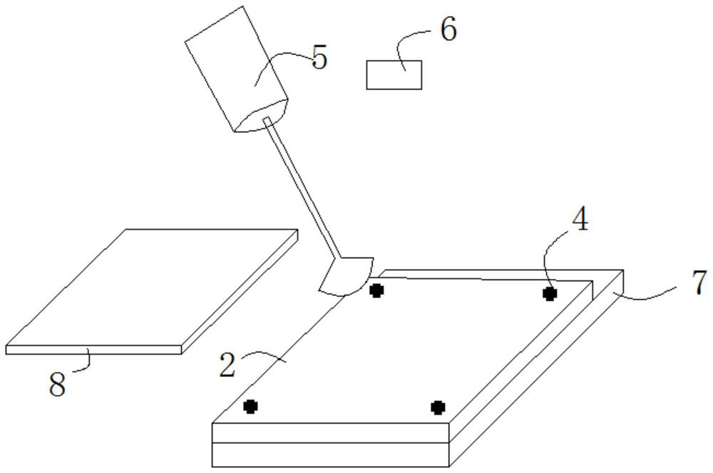
[0039] combine Figure 1-3 , this embodiment provides a bonding method, using the above-mentioned optical components for bonding, the bonding method includes: using infrared light to irradiate the area on the optical adhesive layer 2 provided with alignment marks, and using the identification device 6 to identify the area Shoot to achieve alignment.

[0040]The lamination of the display panel and the touch panel through the optical component is still taken as an example for illustration. That is, the first substrate 7 is the substrate to be bonded on the touch panel. The second substrate 8 is the substrate to be bonded on the display panel. The detailed bonding process is as follows.

[0041] Tear off the light release film, use an infrared light source 5 to irradiate the area where the alignment mark 4 is set, and at the same time use a CCD to capture the alignment mark 4 on the optical adhesive layer 2 and capture the alignment mark 4 on the touch panel , and accordingly...


PUM

PropertyMeasurementUnit
diameteraaaaaaaaaa

Abstract

The invention provides an optical component and its manufacturing method, bonding method and display device, belonging to the field of display technology, which can at least partly solve the alignment accuracy of the existing optical component application and bonding process in the manufacturing process of the display device Not a high question. The optical assembly of the present invention comprises a stacked first release film, an optical adhesive layer and a second release film, and at least one pair A bit mark, the material of the alignment mark includes an up-conversion luminescent material, and the up-conversion luminescent material can convert infrared light into visible light.

Description

technical field [0001] The invention belongs to the field of display technology, and in particular relates to an optical component, a method for manufacturing an optical glue, a bonding method, and a display device. Background technique [0002] Optical adhesives are often used in the field of manufacturing display devices. Usually the optical adhesive is composed of three stacked layers when leaving the factory: heavy release film, optical adhesive layer, and light release film. Alignment marks are made on the heavy release film. Taking the lamination of the display panel and the touch panel as an example, the lamination process using the existing optical adhesive is as follows: tear off the light release film, use CCD to capture the alignment mark on the heavy release film and capture the mark on the touch panel. Alignment marks and attach the optical adhesive layer to the touch panel accordingly; use CCD to capture the alignment marks on the heavy release film and the a...

Claims


Application Information

Patent Timeline
Patent Type & Authority Patents(China)
IPC IPC(8): C09J7/10C09J7/40C09J5/00G09F9/35G09F9/33C09K11/85
CPCC09J5/00C09J2203/318C09K11/7773C09J7/10C09J7/40G09F9/33G09F9/35
Inventor 杨超
Owner BOE TECH GRP CO LTD
Why Eureka
Try Eureka