
Micron light emitting diode matrix display

A light-emitting diode, matrix display technology, applied in the field of visible light communication, can solve the problem of consuming wireless spectrum resources and the like

Pending Publication Date: 2019-08-09
SHENZHEN SITAN TECH CO LTD
View PDF0 Cites 1 Cited by
  • Summary
  • Abstract
  • Description
  • Claims
  • Application Information

AI Technical Summary

Problems solved by technology

Because of the increase in the number of electronic devices, especially people's demand for video services "Anywhere, Anytime", wireless spectrum resources are greatly consumed

Method used


Image

  • Micron light emitting diode matrix display
  • Micron light emitting diode matrix display

Examples


Embodiment 1

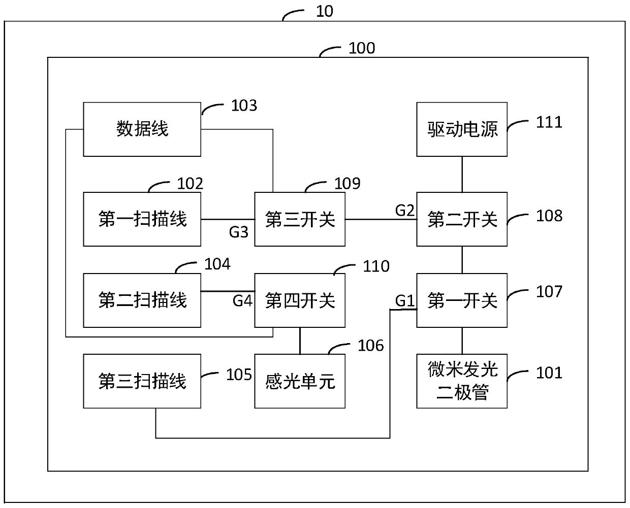
[0032] figure 1 It is a schematic structural diagram of a micron light emitting diode matrix display provided in Embodiment 1 of the present invention, wherein micron light emitting diodes (Micro Light Emitting Diode, micron LED) are used in display elements, and their size is only about 1-100 μm. The micron light-emitting diode matrix display includes multiple pixel circuits, and the drawings of this embodiment are only for illustration, and do not represent the actual number of pixel circuits. This embodiment is applicable to a situation where optical signals can be both transmitted and received.

[0033] Such as figure 1 As shown, the first embodiment provides a micron light-emitting diode matrix display 10, including a plurality of pixel circuits 100, wherein each pixel circuit 100 includes: a micron light-emitting diode 101, the micron light-emitting diode 101 through the first switch 107 and The second switch 108 is connected to the driving power supply 111; the first ...

Embodiment 2

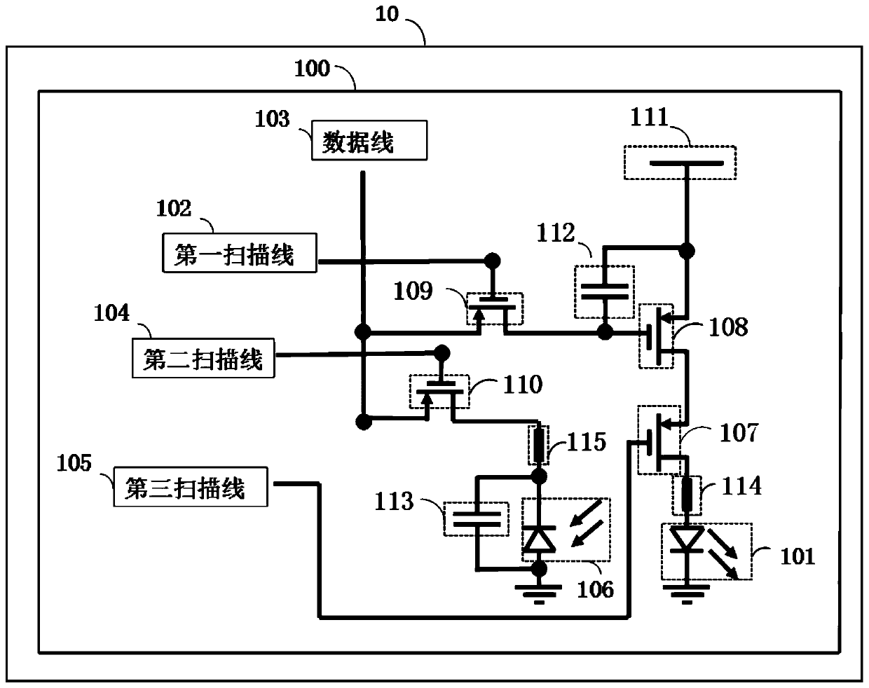
[0038] figure 2 It is a schematic structural diagram of a micron light-emitting diode matrix display provided in Embodiment 2 of the present invention. The technical solution provided in this embodiment is refined on the basis of the above technical solution, and is applicable to scenarios that also include capacitors.

[0039] Such as figure 2 As shown, the micro-LED matrix display 10 includes a plurality of pixel circuits 100 , and each pixel circuit 100 may further include a first capacitor 112 . Wherein, one end of the first capacitor 112 is electrically connected to the source of the second switch, and the other end of the first capacitor 112 is electrically connected to the gate of the second switch, for continuously conducting Pass the second switch.

[0040] Specifically, the first switch 107, the second switch 108, the third switch 109, and the fourth switch 110 may all be PMOS transistors or NMOS transistors. The gates of the MOS transistors correspond to the co...


PUM


Abstract

The embodiment of the invention discloses a micron light-emitting diode matrix display, which comprises a plurality of pixel circuits, wherein each pixel circuit comprises a micron light-emitting diode, and the micron light-emitting diodes are connected to a driving power supply through a first switch and a second switch; a first scanning line connected to the control end of a third switch; a dataline connected to the control end of a second switch through the third switch; a second scanning line connected to the control end of a fourth switch; a third scanning line connected to the control end of the first switch and used for cutting off the first switch at the optical communication receiving time so as to cut off the power supply of the driving power supply to the micrometer light-emitting diode; and a photosensitive unit connected to the data line through the fourth switch so as to transmit a photosensitive signal to the data line when the fourth switch is switched on. According tothe technical scheme provided by the embodiment of the invention, the micrometer light emitting diode and the photosensitive unit are arranged, so that the technical effects of transmitting and receiving optical signals are achieved.

Description

technical field [0001] Embodiments of the present invention relate to visible light communication technology, and in particular to a micron light-emitting diode matrix display. Background technique [0002] With the rapid development of light-emitting diodes, light-emitting diodes are used in many occasions. Visible light communication technology relies on high-speed flashing signals sent by light-emitting diodes to transmit information. [0003] At this stage, the network access technology is usually wireless radio frequency communication. Because of the increase in the number of electronic devices, especially people's demand for video services "Anywhere, Anytime", wireless spectrum resources are greatly consumed. The 380-780nm spectral bandwidth (equivalent to 405THZ) of visible light can be used to alleviate this problem. At this stage, visible light communication technology uses light-emitting diodes as light sources, which can realize both lighting functions and data ...

Claims


Application Information

Patent Timeline
IPC IPC(8): G09G3/32
CPCG09G3/32
Inventor 刘召军李伟增吕志坚范柚攸刘心怡赵晨曦雷雨
Owner SHENZHEN SITAN TECH CO LTD
Learn More