OLED display panel and preparation method thereof

A technology for display panels and substrate substrates, which is used in semiconductor/solid-state device manufacturing, electrical components, and electrical solid-state devices, etc., can solve problems such as increasing the production cycle of OLED devices, and achieve the effect of reducing the production cycle.

Inactive Publication Date: 2019-08-09
WUHAN CHINA STAR OPTOELECTRONICS SEMICON DISPLAY TECH CO LTD
View PDF5 Cites 28 Cited by
  • Summary
  • Abstract
  • Description
  • Claims
  • Application Information

AI Technical Summary

Problems solved by technology

[0004] The invention provides an OLED display panel and a preparation method, which can protect the camera under the display screen from the interference of the cathode translucent film layer, so as to solve the existing liquid crystal display panel. Due to the OLED display panel and the preparation method, the cathode When applied to the under-screen camera technology, two cathode evaporations are required, which increases the technical problems of the production cycle of OLED devices

Method used


Image

  • OLED display panel and preparation method thereof
  • OLED display panel and preparation method thereof
  • OLED display panel and preparation method thereof

Examples


Embodiment Construction

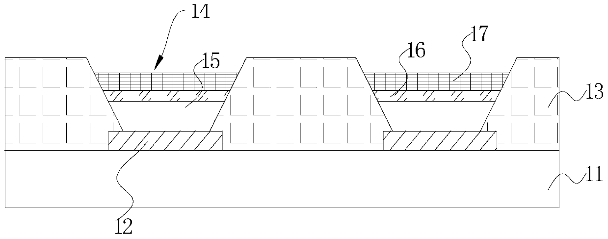
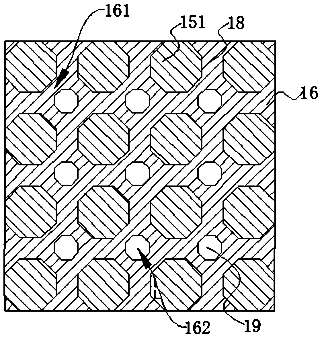
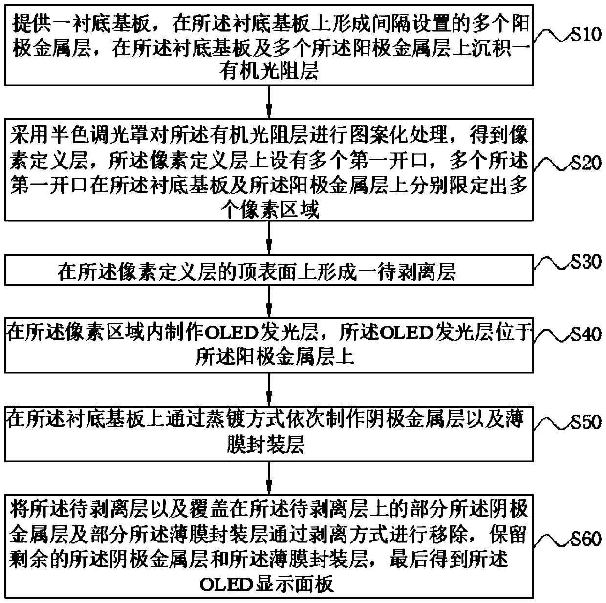
[0031] The following descriptions of the various embodiments refer to the accompanying drawings to illustrate specific embodiments in which the invention may be practiced. The directional terms mentioned in the present invention, such as [top], [bottom], [front], [back], [left], [right], [inside], [outside], [side], etc., are only for reference The orientation of the attached schema. Therefore, the directional terms used are used to illustrate and understand the present invention, but not to limit the present invention. In the figures, structurally similar elements are denoted by the same reference numerals.

[0032] The present invention is aimed at the existing liquid crystal display panel, due to the existing OLED display panel and the preparation method, because when the cathode is applied to the under-screen camera technology, it is necessary to carry out the cathode evaporation twice, which increases the production cycle technology of the OLED device problem, this embo...


PUM


Abstract

The invention provides an OLED display panel and a preparation method thereof. The OLED display panel comprises a substrate, an anode metal layer, a pixel defining layer, OLED light-emitting layers, acathode metal layer and a thin-film encapsulating layer. The pixel defining layer is provided with a plurality of first openings, a plurality of pixel regions are defined on the substrate and the anode metal layer by the multiple first openings, and the OLED light-emitting layers are set in the corresponding pixel regions. The OLED display panel further comprises cathode connection lines, a pattern formed by the cathode metal layer comprises a cathode region and a cathodeless region, the cathode metal layer in the cathode region covers the OLED light-emitting layers and the cathode connectionlines, and the cathodeless region is a plurality of through holes distributed in an array.

Description

technical field [0001] The invention relates to the field of display technology, in particular to an OLED display panel and a preparation method. Background technique [0002] Organic light-emitting diode (OLED) has the advantages of self-luminescence, wide operating temperature range, fast response speed, wide viewing angle, high luminous efficiency, etc., and is known as the next generation of display technology. In small and medium-sized OLED panels, for wider color gamut and better light extraction efficiency, the cathode is designed as a semi-transparent film layer to produce a microcavity effect. The cathode is applied to the OLED side of the CUP (Camera Under Screen) technology, and this translucent film layer will interfere with the camera. In the prior art, in order to avoid such interference, a high-precision metal mask is used to block the cathode, and a specific patterned cathode is generated in the camera area, and then replaced with an ordinary metal mask to f...

Claims


Application Information

Patent Timeline
Patent Type & Authority Applications(China)
IPC IPC(8): H01L27/32H01L51/52H01L51/56
CPCH10K59/122H10K50/822H10K71/00
Inventor 王纯阳高屋雅啓
Owner WUHAN CHINA STAR OPTOELECTRONICS SEMICON DISPLAY TECH CO LTD
Why Eureka
Try Eureka