Vertical ultra low leakage probe card for DC parameter test

A probe card and probe technology, applied in the field of probe cards, can solve problems such as increasing manufacturing costs, and achieve the effects of preventing current leakage, reducing the number of electrical contacts, and reducing manufacturing costs

Inactive Publication Date: 2019-08-09
TEPS CO LTD
View PDF7 Cites 0 Cited by
  • Summary
  • Abstract
  • Description
  • Claims
  • Application Information

AI Technical Summary

Problems solved by technology

[0011] And, as mentioned above, the existing vertical type probe card employs a space transformer that needs to have good mechanical strength and chemical resistance, therefore, there is a problem of increasing the overall manufacturing cost due to the use of the above-mentioned space transformer

Method used


Image

  • Vertical ultra low leakage probe card for DC parameter test
  • Vertical ultra low leakage probe card for DC parameter test
  • Vertical ultra low leakage probe card for DC parameter test

Examples


Embodiment Construction

[0043] Hereinafter, preferred embodiments of the present invention will be described in detail. It should be understood, however, that the detailed description and specific examples, while indicating preferred embodiments of the invention, are illustrative only since various changes and modifications within the spirit and scope of the invention will be suggested to those skilled in the art from the detailed description. Personnel becomes apparent.

[0044] Also, the size and shape of components shown in the drawings referred to in the following detailed description may be exaggerated for convenience and conciseness of description.

[0045] In addition, the terms used herein are defined by considering the functions of the present invention, and may be changed according to user's or operator's habit or purpose. Therefore, definitions of terms should be made based on the entire disclosure set forth herein.

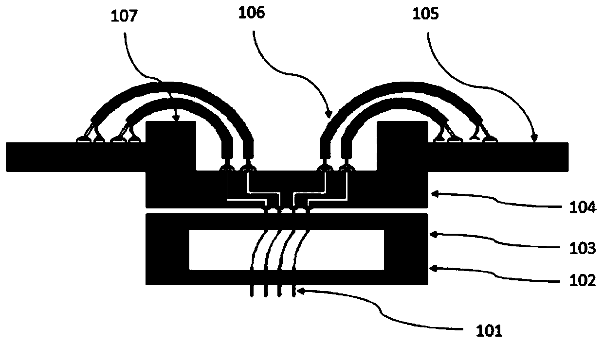
[0046] figure 2is a cross-sectional view showing the structure of a ...


PUM


Abstract

A probe card according to an embodiment of the present invention comprises: a plurality of probes that are in contact with a test target for transmitting an electrical signal; a probe PCB that has a signal line for distributing and transmitting an electrical signal to the plurality of probes; a first guide plate that is arranged to face the test target and that has a plurality of probe holes formed thereon into which ends of the respective plurality of probes are inserted; and a second guide plate that is arranged parallel to the first guide plate, and that has a plurality of probe holes formed thereon into which the other ends of the respective plurality of probes are inserted, wherein the signal line on the probe PCB and the other ends of the respective plurality of probes are directly electrically connected to one another via a coaxial cable.

Description

technical field [0001] The present invention relates to a probe card, more specifically, a vertical probe card capable of handling fine pitches and effectively preventing current leakage. Background technique [0002] In recent years, with the development of the IT industry, semiconductor chips have been widely used in various fields such as computers, mobile phones, monitors, game consoles, home appliances, and automobiles. Before the final step of packaging and mounting in the finished product, this semiconductor chip is subjected to a pre-inspection for evaluating whether it is functioning properly at each step of the manufacturing process to judge whether it is defective. [0003] In the semiconductor inspection step described above, the inspection in the wafer state is performed by inspecting the electrical characteristics of each chip at the wafer level before cutting hundreds to thousands of semiconductor chips formed on the semiconductor wafer into individual chips a...

Claims


Application Information

Patent Timeline
IPC IPC(8): G01R1/073G01R31/28
CPCG01R1/07342G01R31/2863G01R31/2889G01R1/07307
Inventor 李在馥金大原康贤
Owner TEPS CO LTD
Why Eureka
Try Eureka