Substrate processing system used for depositing film
A processing system and a technology for depositing films, applied in the field of substrate processing systems for seamless feature filling
- Summary
- Abstract
- Description
- Claims
- Application Information
AI Technical Summary
Problems solved by technology
Method used
Image

Examples
Embodiment Construction
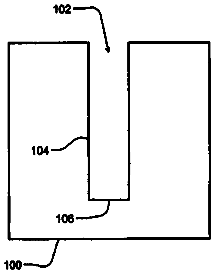
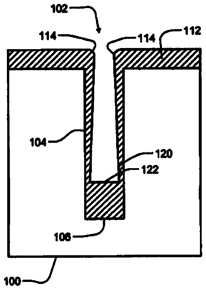
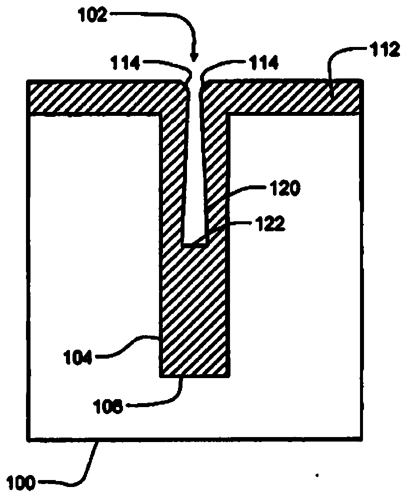
[0067] The present disclosure describes systems and methods for filling features on a substrate. In some embodiments, the features are formed below field regions of the substrate. In some embodiments, seams formed in holes or trenches, such as shallow trench insulators (STIs), during gapfill are eliminated using an atomic layer deposition (ALD) process. Although STI applications have been disclosed, the invention is applicable to other applications requiring feature filling, such as, but not limited to, pre-metal dielectrics, 3D NAND, deep trenches, and the like. The systems and methods described herein enhance bottom-up feature fill during the ALD process by exposing the substrate to a suppressor plasma between at least some of the ALD cycles performed during feature fill.
[0068] In some embodiments, the features are substantially filled by ALD cycles. In other embodiments, the features are not completely filled by the ALD cycle, and other materials are used to fill the f...
PUM
 Abstract
Description
Claims
Application Information
 - Generate Ideas
- Intellectual Property
- Life Sciences
- Materials
- Tech Scout
- Unparalleled Data Quality
- Higher Quality Content
- 60% Fewer Hallucinations
Browse by: Latest US Patents, China's latest patents, Technical Efficacy Thesaurus, Application Domain, Technology Topic, Popular Technical Reports.
© 2025 PatSnap. All rights reserved.Legal|Privacy policy|Modern Slavery Act Transparency Statement|Sitemap|About US| Contact US: help@patsnap.com