Arrangement method of exposure areas on wafer

A technology for exposure area and wafer, which is applied in microlithography exposure equipment, photolithography process exposure device, optics, etc., can solve the problems of wafer edge defocus and improper arrangement, and avoid the problem of wafer edge defocus Effect

Active Publication Date: 2019-08-30
SHANGHAI HUALI INTEGRATED CIRCUTE MFG CO LTD
View PDF4 Cites 4 Cited by
  • Summary
  • Abstract
  • Description
  • Claims
  • Application Information

AI Technical Summary

Problems solved by technology

[0005] In view of the above-mentioned shortcomings of the prior art, the purpose of the present invention is to provide a method for arranging the exposure regions on the wafer, which is used to solve the problem of edge separation of the wafer caused by improper arrangement of the exposure regions on the wafer in the prior art. focus problem

Method used


Image

  • Arrangement method of exposure areas on wafer
  • Arrangement method of exposure areas on wafer
  • Arrangement method of exposure areas on wafer

Examples


Embodiment 1

[0024] like Figure 4 as shown, Figure 4 It is shown as a flowchart of the method for arranging exposure regions on a wafer according to the present invention. The present invention provides a method for arranging exposure regions on a wafer, the method at least including the following steps:

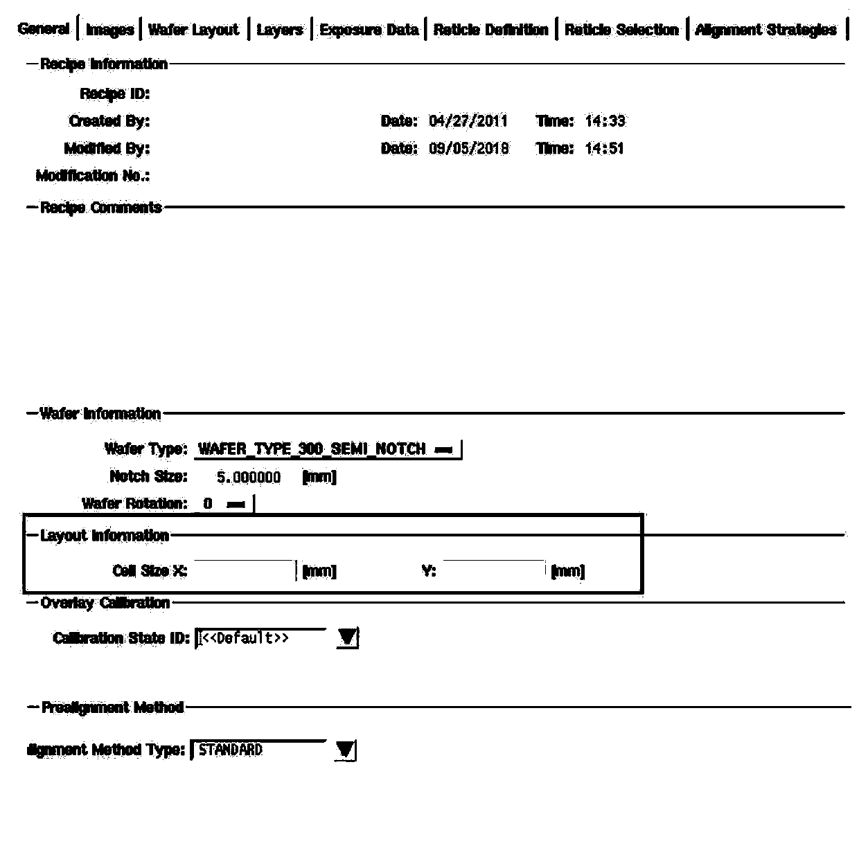
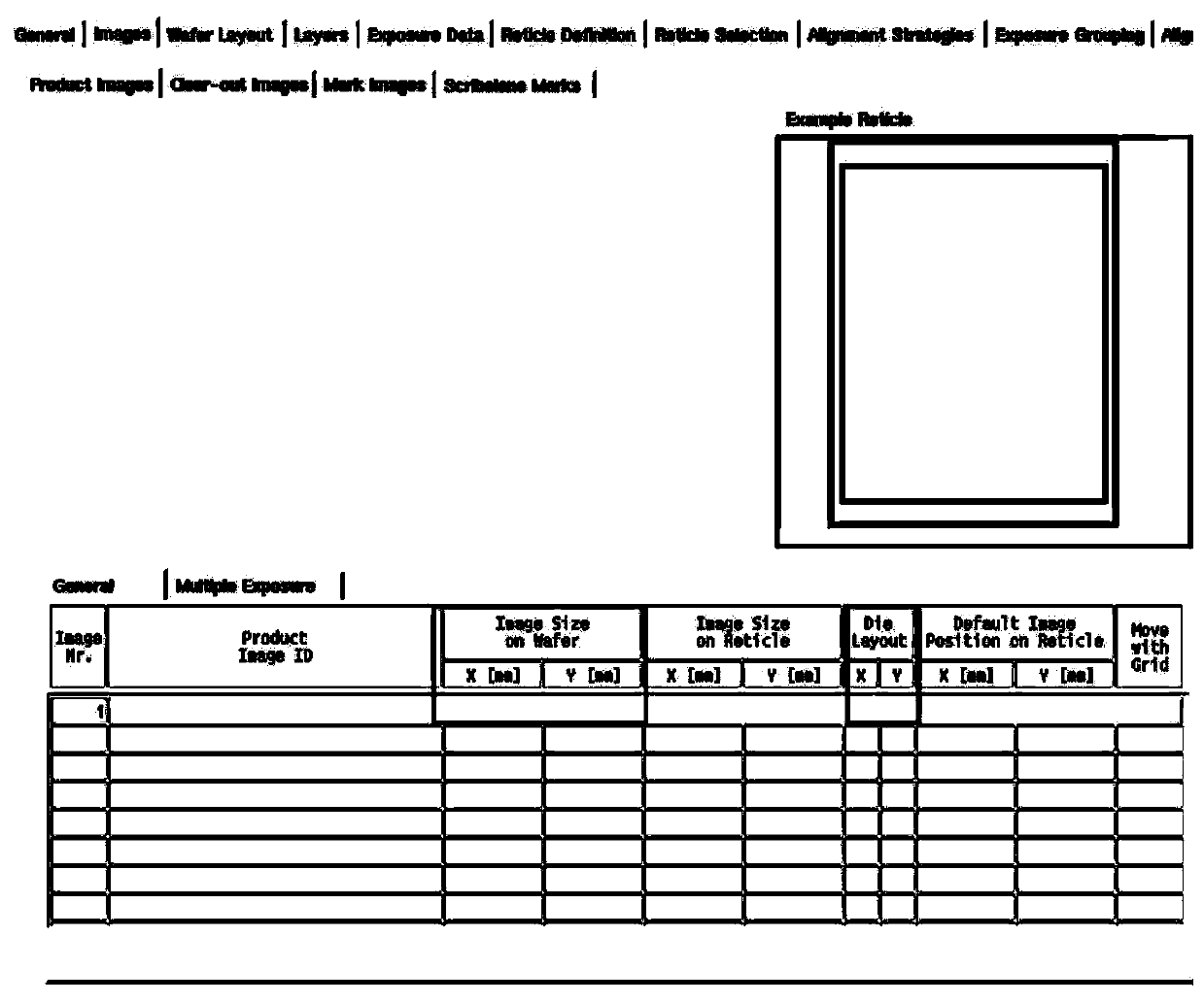
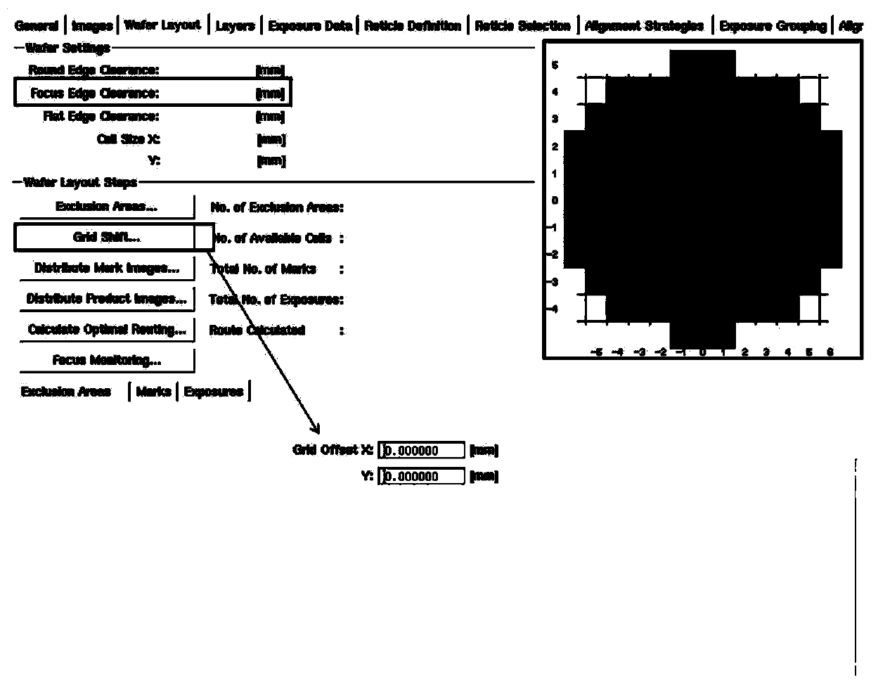
[0025] Step 1. Provide exposure area information and lithography machine exposure information that affects the arrangement of exposure areas; in the lithography process, the maximum range of areas that a lithography machine can support for a single exposure is the exposure area. In the present invention, preferably, the exposure area information in step 1 includes: unit size, exposure area size, and the number of Dies arranged in one exposure area. According to the exposure area, the wafer surface is divided into grids (grid) of several rectangular areas of the same size. The area in each grid is called a unit cell, and there is one exposure area in each unit. The area of ​​the expo...

Embodiment 2

[0033] like Figure 4 as shown, Figure 4 It is shown as a flowchart of the method for arranging exposure regions on a wafer according to the present invention. The present invention provides a method for arranging exposure regions on a wafer, the method at least including the following steps:

[0034] Step 1. Provide exposure area information and lithography machine exposure information that affects the arrangement of exposure areas; in the lithography process, the maximum range of areas that a lithography machine can support for a single exposure is the exposure area. In the present invention, preferably, the exposure area information in step 1 includes: unit size, exposure area size, and the number of Dies arranged in one exposure area. According to the exposure area, the wafer surface is divided into grids (grid) of several rectangular areas of the same size. The area in each grid is called a unit cell, and there is one exposure area in each unit. The area of ​​the expo...


PUM

PropertyMeasurementUnit
widthaaaaaaaaaa

Abstract

The invention provides an arrangement method of exposure areas on a wafer. The arrangement method of exposure areas on a wafer comprises the following steps of: providing exposure area information andphotoetching machine exposure information influencing the arrangement of the exposure area; setting an exposure area rule according to the exposure area information and the photoetching machine exposure information to maximize effective Die; and calculating and obtaining the optimal grid shift and the value of the non-focusing area of the wafer edge by using the exposure area information, the photoetching machine exposure information and the exposure area rule so that the effective Die of the wafer edge is covered. According to the method for intelligently setting the arrangement of the exposure areas on the wafer, three conditions of the size of laser marks, the maximization of effective die and the arrangement of flatness sensors can be comprehensively considered, the optimal arrangement of the exposure areas can be calculated in advance, the problem of defocusing of the edge of the wafer is avoided in advance while the maximization of the effective die is ensured, and the method issuitable for the development trend of advanced technology node photoetching.

Description

technical field [0001] The invention relates to the field of semiconductor manufacturing, in particular to a method for arranging exposure regions on a wafer. Background technique [0002] After coating and baking, the wafer is transferred to the photolithography machine, placed on the wafer table, and exposed according to the specified exposure program. The exposure program of the lithography machine is very rich in content, involving the parameters required for all aspects of exposure, including the arrangement of the exposure area on the wafer, the setting of the exposure area on the mask, how to expose (energy and light conditions), how to Quasi-wafer, what corrections need to be made during exposure, etc. Regarding the layout of the exposure area on the wafer, take a typical lithography machine exposure program as an example, the setting content is as follows Figure 1a , Figure 1b and Figure 1c shown, where Figure 1a Need to set the unit size cell sizeX / Y (that i...

Claims


Application Information

Patent Timeline
Patent Type & Authority Applications(China)
IPC IPC(8): G03F7/20H01L21/027
CPCG03F7/70433H01L21/0274
Inventor 赖璐璐
Owner SHANGHAI HUALI INTEGRATED CIRCUTE MFG CO LTD
Why Eureka
Try Eureka