
Display panel and display device

A display panel and electrode technology, which is used in identification devices, static indicators, instruments, etc., can solve the problems of low-quality fingerprint imaging under the screen and high pixel circuit density.

Active Publication Date: 2019-08-30
KUNSHAN GO VISIONOX OPTO ELECTRONICS CO LTD
View PDF9 Cites 14 Cited by
  • Summary
  • Abstract
  • Description
  • Claims
  • Application Information

AI Technical Summary

Problems solved by technology

[0004] However, with the continuous improvement of display requirements, the pixel density (Pixels Per Inch, PPI for short) and pixel circuit density of the display panel are relatively high, which causes the light reflected to the fingerprint recognition unit to be blocked during fingerprint recognition, and the fingerprint recognition under the screen is blocked. Overall image quality is poor

Method used


Image

  • Display panel and display device
  • Display panel and display device
  • Display panel and display device

Examples


Embodiment Construction

[0027] In order to make the purposes, technical solutions and advantages of the embodiments of the present invention clearer, the technical solutions in the embodiments of the present invention will be clearly and completely described below with reference to the accompanying drawings in the embodiments of the present invention. Obviously, the described embodiments It is only a part of the embodiments of the present invention, but not all of the embodiments. Based on the embodiments of the present invention, all other embodiments obtained by those of ordinary skill in the art without creative efforts shall fall within the protection scope of the present invention.

[0028] In addition, the terms "first" and "second" are only used for descriptive purposes, and should not be construed as indicating or implying relative importance or implying the number of indicated technical features. Thus, a feature defined as "first" or "second" may expressly or implicitly include one or more o...


PUM


Abstract

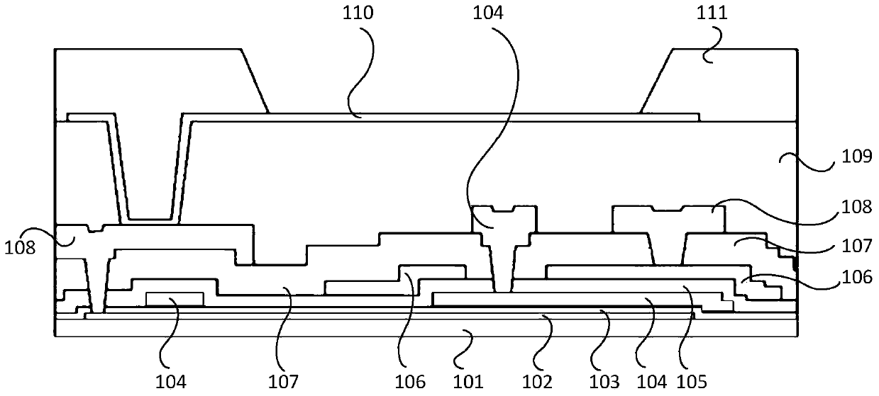
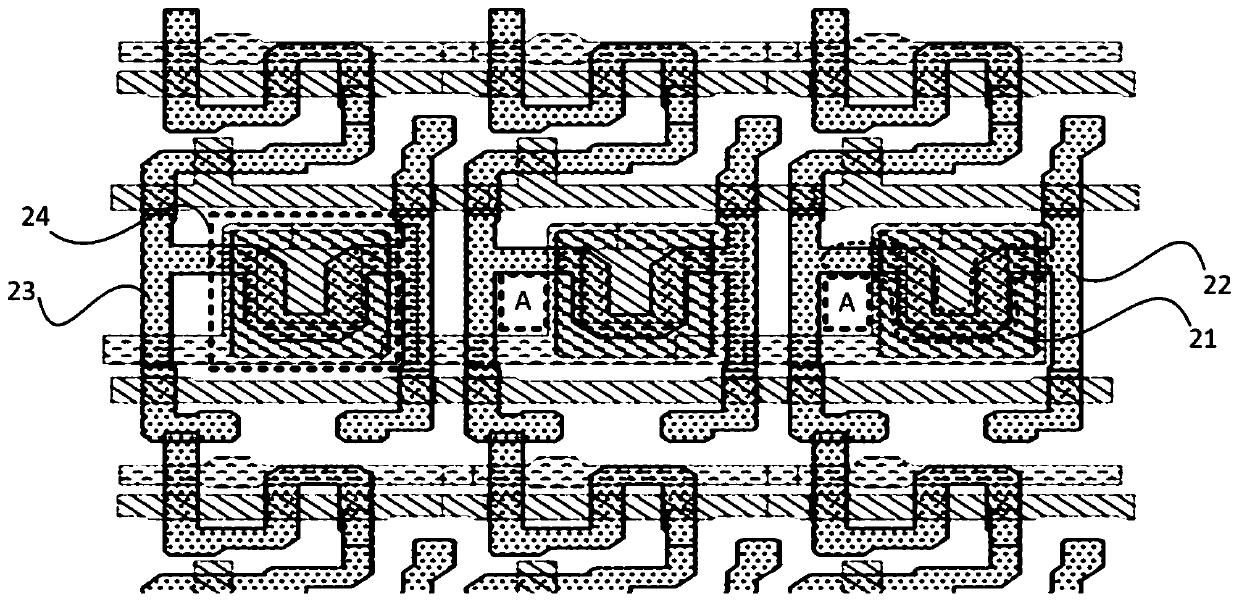
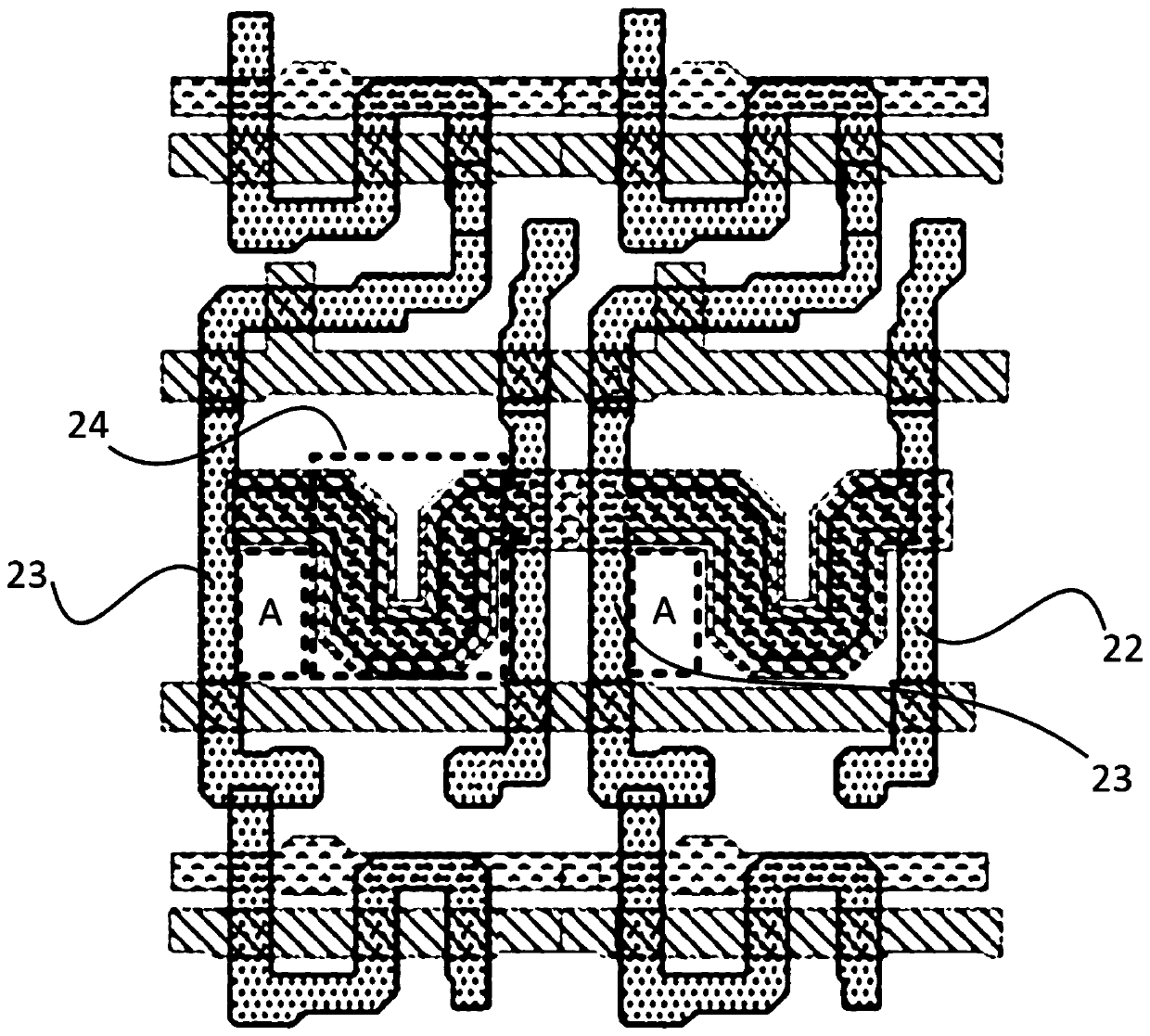
The invention provides a display panel and a display device, being characterized in that a fingerprint identification area of the display panel comprises a substrate layer and a pixel circuit; the pixel circuit comprises a DTFT unit, a source electrode wire, a drain electrode wire and a capacitor unit which are arranged on the substrate layer; a source region of the DTFT unit is connected with thesource electrode wire; a drain region of the DTFT unit is connected with the drain electrode wire, and a light transmitting region is arranged between a channel region of the DTFT unit and the drainelectrode wire; the projection of the channel region of the DTFT unit on the substrate layer and the projection of the channel region close to the source electrode wire on the substrate layer reduce the width of a gap between the channel region of the DTFT unit and the source electrode wire and increase the distance between the channel region of the DTFT unit and the drain electrode wire, so thatthe light transmission area of a single light transmission region is increased; and the projection of the capacitor unit on the substrate layer covers the projection of the channel region on the substrate layer, so that diffraction of a gap between the channel region and the source electrode wire is reduced, and the under-screen fingerprint imaging quality is improved.

Description

technical field [0001] The present invention relates to the field of display technology, and in particular, to a display panel and a display device. Background technique [0002] With the development of display technology, in order to improve the user experience, by reusing the display area of ​​the display panel as the fingerprint identification area, fingerprint identification under the screen can be realized. When a user performs a fingerprint identification operation on a display device with an off-screen fingerprint identification function, the display device can detect the user's fingerprint information by simply touching the finger on the fingerprint identification area of ​​the display screen. [0003] In the display panel in the prior art, the way of realizing the fingerprint recognition under the screen is usually that a fingerprint recognition unit is embedded in the substrate of the display panel. During fingerprint recognition, the user's finger touches the sur...

Claims


Application Information

Patent Timeline
IPC IPC(8): G06K9/20G06K9/22G06K9/24G09F9/00G09G3/20G06V10/12G06V10/147
CPCG09G3/20G09F9/00G06V10/17G06V10/12G06V10/147H01L27/14678G06V40/1318H01L27/1222H01L27/124H10K59/1216H10K59/131H01L25/167H01L27/1218H01L27/1255H01L27/156
Inventor 秦旭宋艳芹李威龙张露
Owner KUNSHAN GO VISIONOX OPTO ELECTRONICS CO LTD
Learn More