Method for detecting printed circuit board

A technology for printed circuit boards and detection methods, which is applied to electronic circuit testing, electrical measurement, and measurement devices, etc., can solve the problems of printed circuit board layout without unified standardized documents, complex printed circuit board structure, increased time cost and inspection cost, etc.

Inactive Publication Date: 2019-09-17
AMOLOGIC (SHANGHAI) CO LTD
View PDF11 Cites 1 Cited by
  • Summary
  • Abstract
  • Description
  • Claims
  • Application Information

AI Technical Summary

Problems solved by technology

[0002] With more and more functions and higher performance requirements of electronic products, the requirements for printed circuit boards are also higher and higher. Therefore, engineers are required to detect the layout of printed circuit boards according to the layout principles of printed circuit boards. However, At present, there is no unified standardized document for the layout of printed circuit boards, and the structure of printed circuit boards is complex
[0003] In the current existing technology, engineers usually inspect the printed circuit board. However, due to the different focus of each engineer, the engineer may not inspect several inspection points of the printed circuit board, resulting in the inability to inspect the entire printed circuit board. Therefore, multiple inspections are required to achieve a comprehensive inspection of the entire printed circuit board, which increases the time cost and inspection cost, and even affects the development progress of the entire electronic product

Method used


Image

  • Method for detecting printed circuit board

Examples


Embodiment Construction

[0048] The following will clearly and completely describe the technical solutions in the embodiments of the present invention with reference to the accompanying drawings in the embodiments of the present invention. Obviously, the described embodiments are only some, not all, embodiments of the present invention. Based on the embodiments of the present invention, all other embodiments obtained by persons of ordinary skill in the art without creative efforts fall within the protection scope of the present invention.

[0049] It should be noted that, in the case of no conflict, the embodiments of the present invention and the features in the embodiments can be combined with each other.

[0050] The present invention will be further described below in conjunction with the accompanying drawings and specific embodiments, but not as a limitation of the present invention.

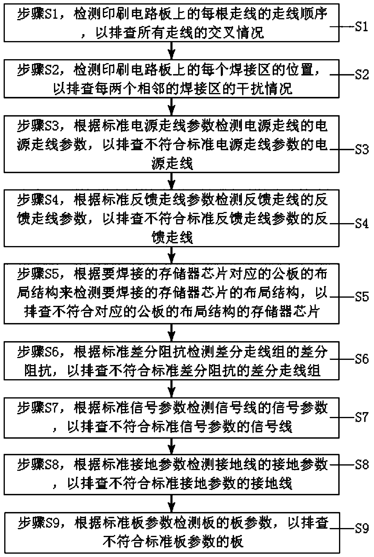
[0051] The invention includes a detection method of a printed circuit board, wherein a detection list is provide...


PUM


Abstract

The inventors provide a method for detecting a printed circuit board, and the method provides a detection list set with detecting steps, and detects the printed circuit board by the detecting steps. The method provided by the invention has the beneficial effects that each detection point is sequentially detected according to the detecting steps, thereby realizing the overall detection of the entire printed circuit board, saving the detection time, and further accelerating the adjustment progress of the printed circuit board.

Description

technical field [0001] The invention relates to the field of printed circuit boards, in particular to a detection method for printed circuit boards. Background technique [0002] With more and more functions and higher performance requirements of electronic products, the requirements for printed circuit boards are also higher and higher. Therefore, engineers are required to detect the layout of printed circuit boards according to the layout principles of printed circuit boards. However, At present, there is no unified standardized document for the layout of printed circuit boards, and the structure of printed circuit boards is complex. [0003] In the current existing technology, engineers usually inspect the printed circuit board. However, due to the different focus of each engineer, the engineer may not inspect several inspection points of the printed circuit board, resulting in the inability to inspect the entire printed circuit board. Therefore, multiple inspections are...

Claims


Application Information

Patent Timeline
Patent Type & Authority Applications(China)
IPC IPC(8): G01R31/28G01R1/04
CPCG01R1/04G01R31/2851
Inventor 肖运涓张坤黄敏君
Owner AMOLOGIC (SHANGHAI) CO LTD
Why Eureka
Try Eureka