Check patentability & draft patents in minutes with Patsnap Eureka AI!

Modulation processing device and method

A modulation processing and processor technology, applied in the computer field, can solve problems such as difficulty in completing the reading and processing of data to be modulated, and achieve the effects of quick reading processing, optimizing modulation processing methods, and improving query efficiency

Active Publication Date: 2019-10-08
上海思朗科技有限公司
View PDF9 Cites 1 Cited by
  • Summary
  • Abstract
  • Description
  • Claims
  • Application Information

AI Technical Summary

Problems solved by technology

However, when the modulation order cannot be divisible by 8, for example, when the modulation order is 6, it is difficult to complete the reading process of the data to be modulated by using a single command at this time.
Therefore, in the case that the modulation order cannot be divisible by 8, the modulation processing method in the prior art cannot conveniently and quickly complete the reading processing of the data to be modulated

Method used


Image

  • Modulation processing device and method
  • Modulation processing device and method
  • Modulation processing device and method

Examples


Embodiment Construction

[0026] Exemplary embodiments of the present disclosure will be described in more detail below with reference to the accompanying drawings. Although exemplary embodiments of the present disclosure are shown in the drawings, it should be understood that the present disclosure may be embodied in various forms and should not be limited by the embodiments set forth herein. Rather, these embodiments are provided for more thorough understanding of the present disclosure and to fully convey the scope of the present disclosure to those skilled in the art.

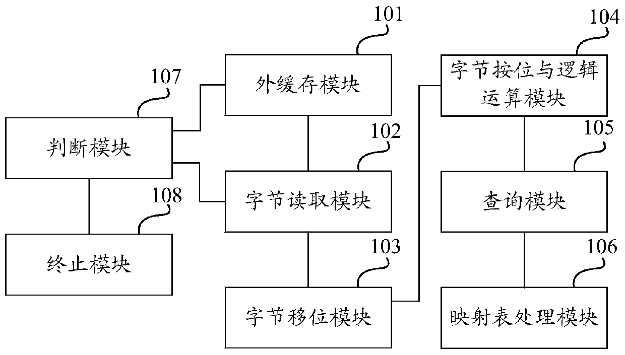
[0027] figure 1 shows a structural block diagram of a modulation processing device according to an embodiment of the present invention, such as figure 1 As shown, the device includes: an external cache module 101 , a byte read module 102 , a byte shift module 103 , a byte bitwise AND logic operation module 104 and a query module 105 .

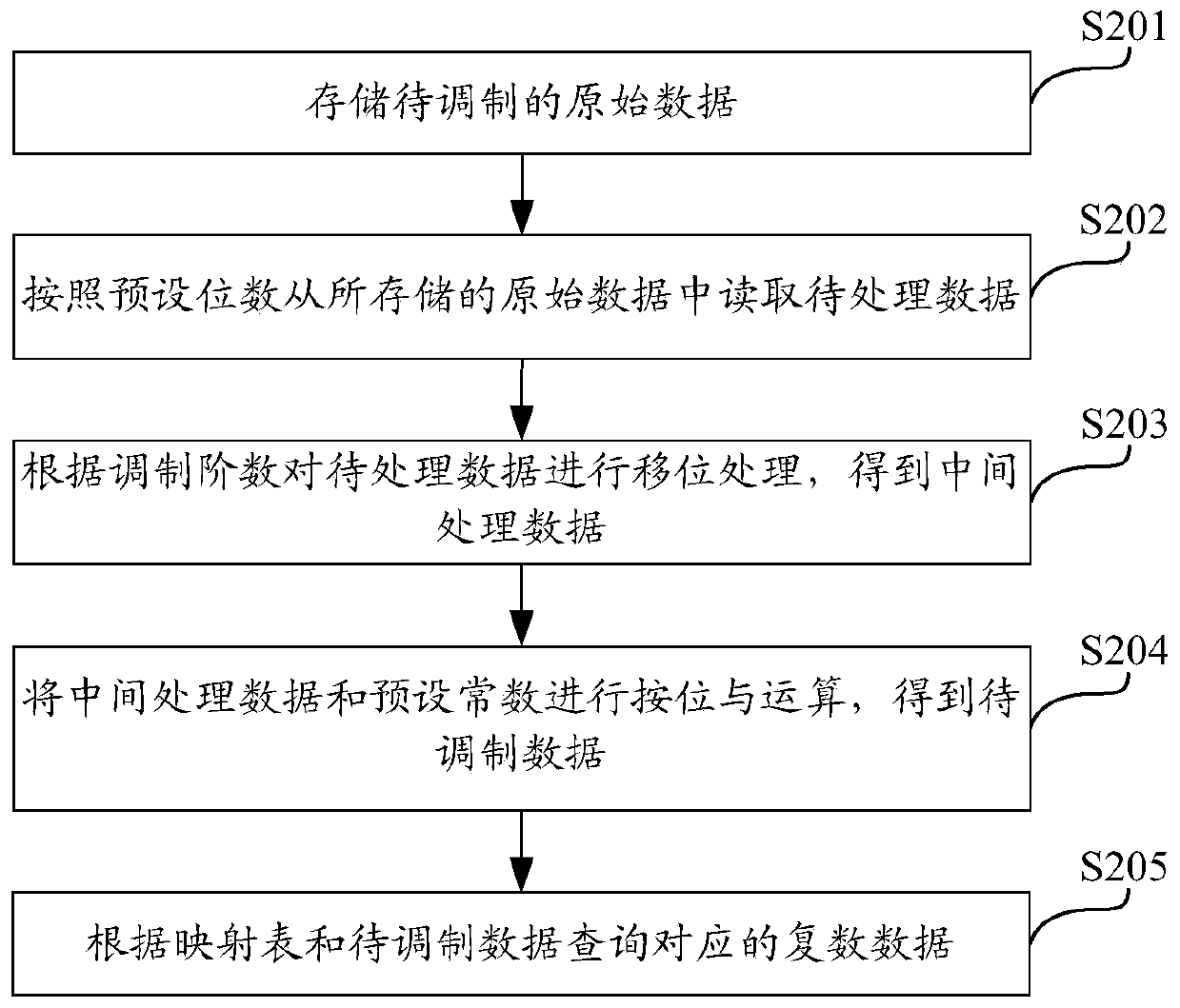
[0028] The external buffer module 101 is used for: storing the original data to be modulated. ...


PUM


Abstract

The invention discloses a modulation processing device and method. The modulation processing device comprises an external caching module which is used for storing to-be-modulated original data, a bytereading module which is used for reading to-be-processed data from the original data stored in the external caching module according to a preset bit, a byte shift module which is used for performingshift processing on the to-be-processed data according to the modulation order to obtain intermediate processing data, a byte bitwise AND logic operation module which is used for performing bitwise AND operation on the intermediate processing data and a preset constant to obtain to-be-modulated data, and a query module which is used for querying the corresponding complex data according to the mapping table and the to-be-modulated data. According to the technical scheme, bit can be used as an operation unit for modulation processing, and bit-level reading processing of to-be-modulated data is effectively achieved, and complex number data corresponding to the to-be-modulated data are inquired in combination with the mapping table, and the inquiry efficiency of the complex number data is effectively improved, and the modulation processing efficiency is greatly improved.

Description

technical field [0001] The invention relates to the field of computer technology, in particular to a modulation processing device and method. Background technique [0002] Based on the communication protocol, modulation essentially maps every continuous bit in the binary data to a complex number data, where the continuous number of bits is called the modulation order. For example, in QPSK (Quadrature Phase Shift Keying, Quadrature PhaseShift Keying) modulation, every continuous 2 bits in binary data are mapped to a complex number data, and its modulation order is 2; in 64QAM (phase quadrature amplitude modulation , Quadrature Amplitude Modulation) modulation, each continuous 6 bits in the binary data is mapped to a complex number data, and its modulation order is 6. [0003] According to the communication protocol, the current typical modulation orders are 1, 2, 4, 6, 8, etc., while most of the assembly instruction sets of existing processors use bytes as the operation unit...

Claims


Application Information

Patent Timeline
IPC IPC(8): G06F5/01G06F7/57H04L27/00
CPCG06F5/015G06F7/57H04L27/00
Inventor 孙一松李桓郭晨王东琳
Owner 上海思朗科技有限公司
Features
  • R&D
  • Intellectual Property
  • Life Sciences
  • Materials
  • Tech Scout
  • Unparalleled Data Quality
  • Higher Quality Content
  • 60% Fewer Hallucinations
Learn More