Circuit board electroplating method

A circuit board and selective plating technology, which is applied in the direction of electrical components, printed circuits, printed circuit manufacturing, etc., can solve the problems of differences in copper sinking rate, increase in production costs, and difficulty in post-processing, so as to achieve good plating uniformity and save energy. The effect of consistent electroplating cost and electroplating parameters

Inactive Publication Date: 2019-10-18
SHENZHEN SUNWAY COMM
View PDF4 Cites 0 Cited by
  • Summary
  • Abstract
  • Description
  • Claims
  • Application Information

AI Technical Summary

Problems solved by technology

[0002] With the development of electronic products, the requirements for the electrical performance and folding resistance of circuit boards are getting higher and higher. Therefore, circuit boards are mostly electroplated by selective plating, such as figure 1 and figure 2 Shown, when selecting plating, usually front side and back side select plating area to be different, there is following shortcoming: 1, by adjusting the area of ​​non-select plating area, make the select plating area of ​​two sides equal (as image 3 shown), which will lead to uneven copper plating on the surface copper and hole copper (such as Figure 4 As shown), the post-process (etching) is very difficult; 2. By reducing the area of ​​the non-selective plating area on the front, the area of ​​the selective plating area on both sides is equal, which will increase the production cost; 3. Adjust the current density of the front and back through the equipment, the current When the density is different, the copper ions are affected by different currents in the copper plating tank, which will lead to differences in the copper deposition rate, resulting in uneven copper plating.

Method used


Image

  • Circuit board electroplating method
  • Circuit board electroplating method
  • Circuit board electroplating method

Examples


Embodiment 1

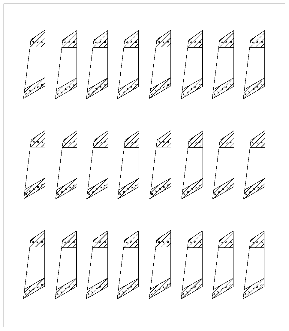
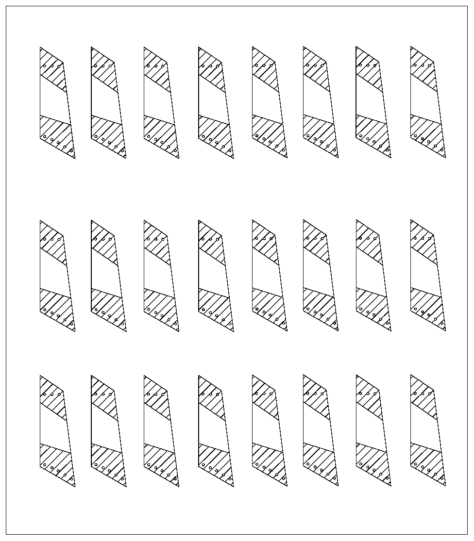
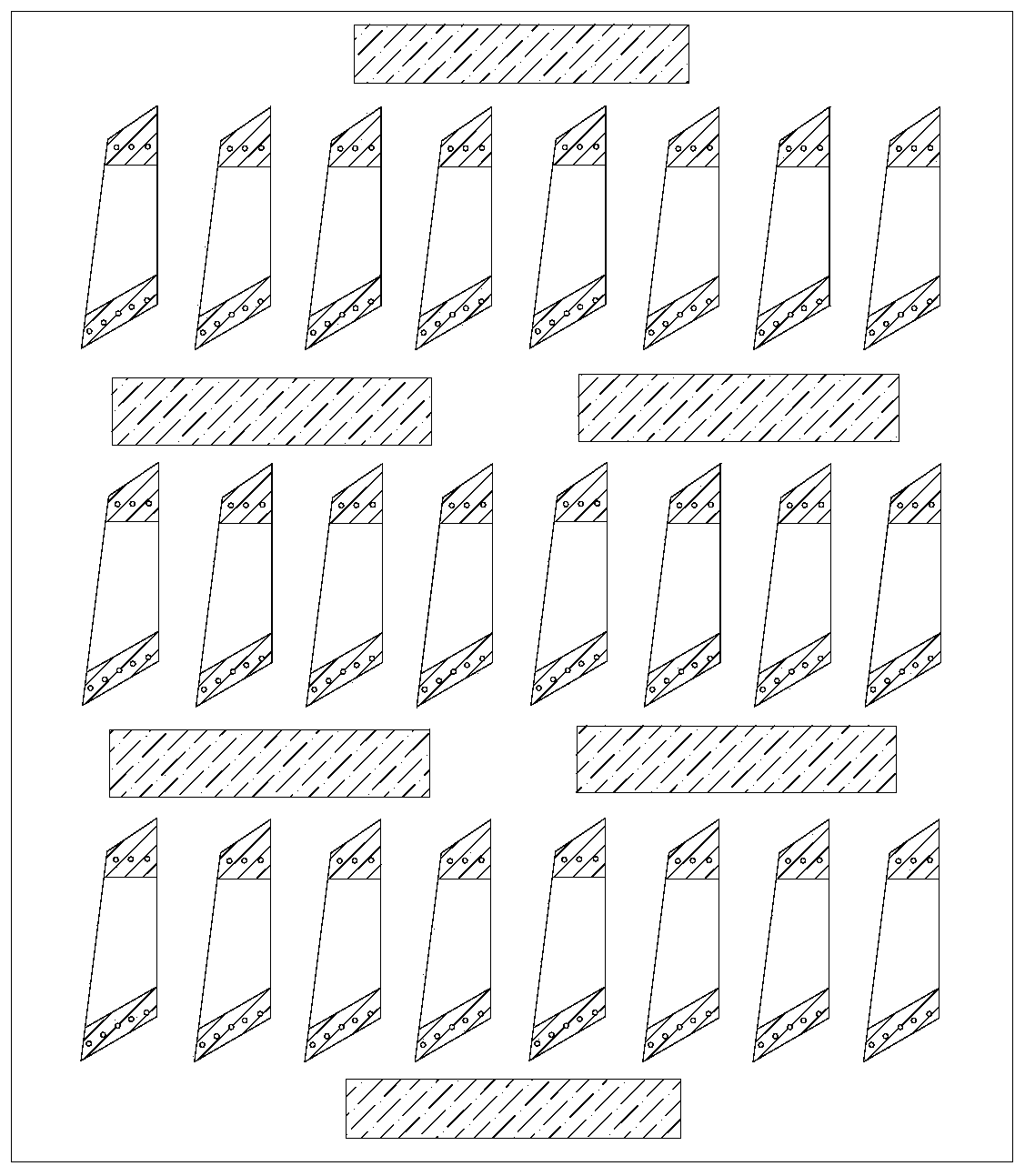
[0032] Please refer to Figure 5 to Figure 7 , Embodiment 1 of the present invention is:

[0033] A circuit board electroplating method, comprising the steps of:

[0034] 1) Obtain the front selective plating area 11 and the rear selective plating area 12 of a single product 1 respectively. Generally, the areas of the selective plating area 11 on the front side and the selective plating area 12 on the back side are different. In this embodiment, it is assumed that the area of ​​the front selective plating area 11 is 20% of the area (single side) of a single product 1, and the area of ​​the back selective plating area 12 is 40% of the area of ​​a single product 1 (single side).

[0035] 2) When the areas of the front selective plating area 11 and the rear selective plating area 12 are different, the raw materials for making a single product 1 are arranged in a selective plating area so that the adjacent two individual products 1 in the same row The selective plating areas 11...


PUM


Abstract

The invention discloses a circuit board electroplating method. The circuit board electroplating method comprises steps that a front selective plating region and a back selective plating region of a single product are separately obtained; when the areas of the front selective plating region and the back selective plating region are different, a raw material for making the single product is subjected to selective plating region arrangement, the front selective plating regions of adjacent two single products located in the same row are respectively located on two sides of the raw material, and the total areas of the selective plating regions of the two sides of the raw material are the same, and the raw material is electroplated according to selective plating region arrangement. The circuit board electroplating method is advantaged in that the area of non-selective plating regions of the raw material is not needed, plating parameters on the two sides of the raw material are the same, plating uniformity is good, and plating cost can be saved.

Description

technical field [0001] The invention relates to the technical field of electroplating, in particular to a circuit board electroplating method. Background technique [0002] With the development of electronic products, the requirements for the electrical performance and folding resistance of circuit boards are getting higher and higher. Therefore, circuit boards are mostly electroplated by selective plating, such as figure 1 and figure 2 Shown, when selecting plating, usually front side and back side select plating area to be different, there is following shortcoming: 1, by adjusting the area of ​​non-select plating area, make the select plating area of ​​two sides equal (as image 3 shown), which will lead to uneven copper plating on the surface copper and hole copper (such as Figure 4 As shown), the post-process (etching) is very difficult; 2. By reducing the area of ​​the non-selective plating area on the front, the area of ​​the selective plating area on both sides is...

Claims


Application Information

Patent Timeline
IPC IPC(8): H05K3/18
CPCH05K3/18H05K2203/0723
Inventor 余辉李绪东虞成城张辉谈兴
Owner SHENZHEN SUNWAY COMM
Why Eureka
Try Eureka