
SPI flash burner

A burner and circuit technology, applied in the field of code burning, can solve problems such as delayed debugging time, reverse chip placement, chip burning damage, etc., so as to save time and waste and improve work efficiency

Active Publication Date: 2019-11-12
SHENZHEN NETCOM ELECTRONICS CO LTD
View PDF3 Cites 1 Cited by
  • Summary
  • Abstract
  • Description
  • Claims
  • Application Information

AI Technical Summary

Problems solved by technology

[0002]SPI NOR / NAND flash (hereinafter referred to as flash), as a code storage chip, is widely used in various products on the market. Generally, the flash chip is pasted on the Before printing the circuit board, it needs to be burned in advance. In the product development stage, R&D personnel frequently use the programmer to burn the code. The easy mistake is to put the chip upside down. Some programmers will prompt the chip If it is misplaced, the developer needs to power off the programmer and re-place the chip, which greatly delays the debugging time, and on some programmers with insufficient protection measures, the chip may even be burned directly.

Method used


Image

  • SPI flash burner
  • SPI flash burner
  • SPI flash burner

Examples


Embodiment Construction

[0023] The present invention will be further described below in conjunction with accompanying drawing:

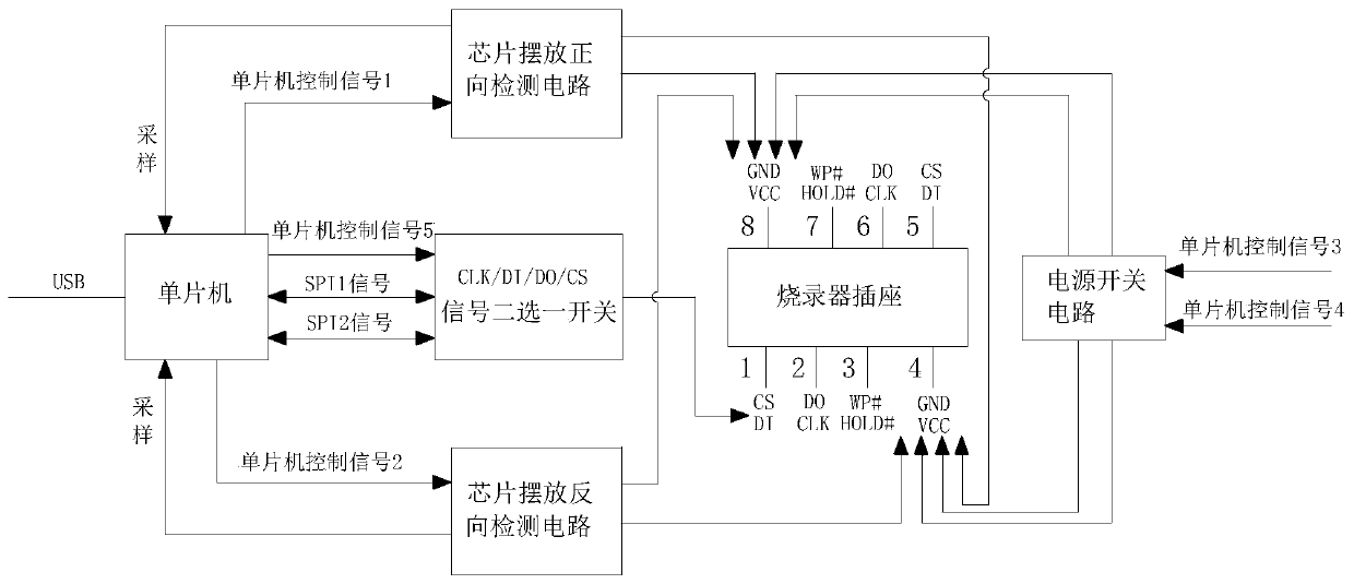
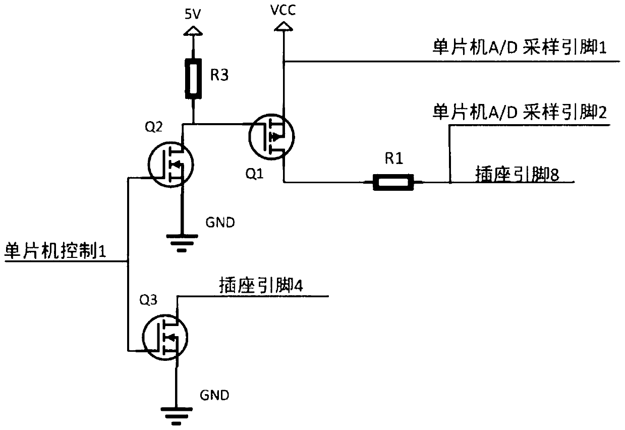
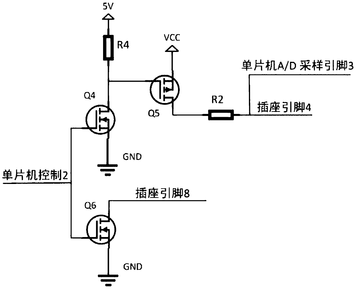
[0024] Such as figure 1 As shown, the present invention includes a single-chip microcomputer, a switch for selecting one of two signals, a chip placement forward detection circuit, a chip placement reverse detection circuit, a burner socket and a power switch circuit, and the power switch circuit is provided with two control signal input terminals ;

[0025] The single-chip microcomputer is provided with a USB interface for communicating with the computer, and its first control signal output terminal is connected to the control signal input terminal of the chip placement forward detection circuit, and its second control signal output terminal is connected to the chip placement reverse detection circuit. The control signal input terminal is connected, the third control signal output terminal is connected to one of the control signal input terminals of the power switch circu...


PUM


Abstract

The invention discloses an SPI flash burner. The SPI flash burner comprises a single-chip microcomputer, a one-out-of-two signal switch, a chip placement forward detection circuit, a chip placement reverse detection circuit, a burner socket and a power switch circuit. The chip placement detection circuit is additionally arranged in the burner equipment, so that chip burning can be carried out no matter whether a chip is placed forwards or reversely, unnecessary time waste of engineers in the debugging process is reduced, and the working efficiency is improved.

Description

technical field [0001] The invention belongs to the technical field of code burning, and in particular relates to an SPI flash burning device. Background technique [0002] SPI NOR / NAND flash (hereinafter referred to as flash), as a code storage chip, is widely used in various products on the market. Generally, before attaching the flash chip to the printed circuit board, it needs to be programmed in advance. In the product In the development stage, R&D personnel frequently use the programmer to burn codes. The most common mistake is to put the chip upside down. Some programmers will prompt that the chip is misplaced. The developer needs to power off the programmer and re-place it. The chip greatly delays the debugging time, and on some burners with insufficient protection measures, the chip may even be burned directly. Contents of the invention [0003] The purpose of the present invention is just to provide a kind of SPI flash burner in order to solve the above problems...

Claims


Application Information

Patent Timeline
Patent Type & Authority Applications(China)
IPC IPC(8): G06F8/61G06F13/40
CPCG06F8/63G06F13/4022
Inventor 李威
Owner SHENZHEN NETCOM ELECTRONICS CO LTD
Learn More