Waveform signal detection method and device

A waveform signal and detection method technology, applied in the circuit field, can solve problems such as low verification efficiency and complicated operation, and achieve the effect of avoiding complicated operation and improving verification efficiency

Active Publication Date: 2021-06-22
SHENZHEN GOODIX TECH CO LTD
View PDF17 Cites 0 Cited by
  • Summary
  • Abstract
  • Description
  • Claims
  • Application Information

AI Technical Summary

Problems solved by technology

[0004] In view of this, one of the technical problems solved by the embodiments of the present invention is to provide a waveform signal detection method and device to overcome the problem of verifying the modules in the chip that output waveforms through I / O pins in the prior art. When, the operation is complicated and the verification efficiency is low

Method used


Image

  • Waveform signal detection method and device
  • Waveform signal detection method and device
  • Waveform signal detection method and device

Examples


Embodiment 1

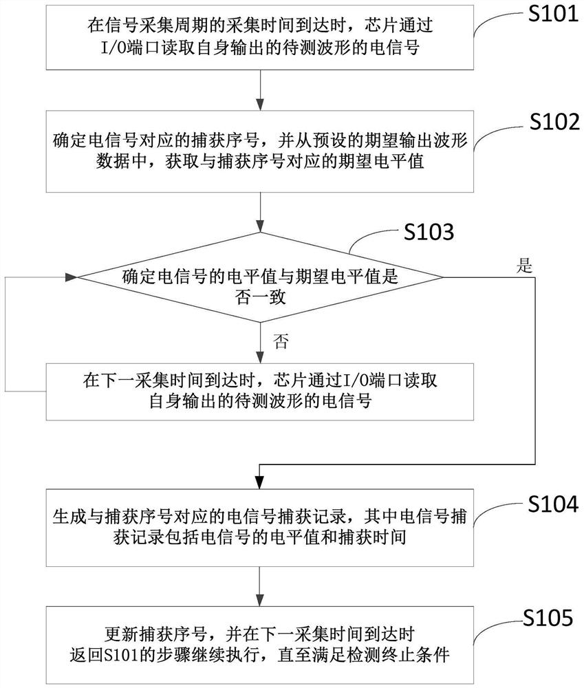
[0017] figure 1 A schematic flowchart of a method for detecting a waveform signal according to an embodiment of the present invention is shown. like figure 1 As shown, the waveform signal detection method includes:

[0018] S101: When the acquisition time of the signal acquisition cycle arrives, the chip reads the electrical signal of the waveform to be measured output by itself through the I / O port.

[0019] When testing the chip, especially some modules inside the chip that can output waveforms through the I / O port (for example, PWM modules), you can determine whether the output waveform of the I / O port conforms to the expected waveform, so as to determine the tested module meets the requirements.

[0020] The chip includes at least one I / O port, and the functional modules in the chip are electrically connected to these I / O ports, so that electrical signals can be read in or output through these I / O ports.

[0021] In order to obtain the waveform output by the I / O port, ...

Embodiment 2

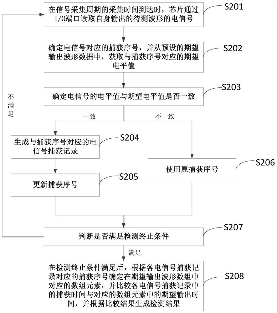
[0037] figure 2 A schematic flowchart of a method for detecting a waveform signal according to Embodiment 2 of the present invention is shown. like figure 2 As shown, the waveform signal detection method includes:

[0038] S201: When the acquisition time of the signal acquisition period arrives, the chip reads the electrical signal of the waveform to be measured output by itself through the I / O port.

[0039] In a feasible way, when the chip reads the electrical signal of the waveform to be measured output by itself through the I / O port (that is, the I / O pin), the chip can directly output the electrical signal of the waveform to be measured through the I / O port. The electrical signal is read back.

[0040] In this case, the I / O port that outputs the electrical signal of the waveform to be measured can be configured as an I / O pin floating, pulled up or pulled down. In this way, there is no need to set additional I / O ports or pins , saving chip implementation cost.

[004...

Embodiment 3

[0080] like Figure 4 As shown, a structural block diagram of a waveform signal detection device according to Embodiment 3 of the present invention is shown.

[0081] The waveform signal detection device of this embodiment includes: an electrical signal acquisition module 401, which is used to read the electrical signal of the waveform to be measured output by the chip through the I / O port when the acquisition time of the signal acquisition cycle arrives; the expected level value The determination module 402 is used to determine the capture sequence number corresponding to the electrical signal, and obtains the expected level value corresponding to the capture sequence number from the preset expected output waveform data; the level value comparison module 403 is used to determine the electrical signal of the electrical signal Whether the average value is consistent with the expected level value; the capture record generation module 404 is used to generate an electrical signal ...


PUM


Abstract

Embodiments of the present invention provide a waveform signal detection method and device. The waveform signal detection method includes that when the acquisition time of the signal acquisition period arrives, the chip reads the electrical signal of the waveform to be measured output by itself through the I/O port; determines the capture sequence number corresponding to the electrical signal, and outputs the waveform from the preset expectation In the data, the expected level value corresponding to the capture sequence number is obtained; if the level value of the electrical signal is consistent with the expected level value, an electrical signal capture record corresponding to the capture sequence number is generated, wherein the electrical signal capture record includes the electrical signal Level value and capture time; update the capture sequence number, and when the next capture time arrives, the step of returning to the chip to read the electrical signal of the waveform to be measured output by itself through the I/O port continues until the detection termination condition is met. The waveform signal detection method can overcome the defects of complex operation and low verification efficiency when verifying a module in a chip that outputs a waveform through an I/O pin.

Description

technical field [0001] Embodiments of the present invention relate to the field of circuit technology, and in particular, to a waveform signal detection method and device. Background technique [0002] When performing functional verification on the chip from the software level, for modules that can output waveforms through I / O (Input / Output, input / output) pins, such as PWM modules (Pulse Width Modulation, pulse width modulation modules), GPIO modules (General Purpose Input Output, general-purpose input / output module), etc., the common method of verification is to connect external test equipment such as oscilloscope or logic analyzer to the I / O pin, cooperate with the third-party software tool supporting the oscilloscope or logic analyzer, and display the oscilloscope Or the waveform output by the I / O pin captured by the logic analyzer. By observing or measuring the waveform output by the oscilloscope or logic analyzer, comparing it with the expected output waveform, etc., t...

Claims


Application Information

Patent Timeline
Patent Type & Authority Patents(China)
IPC IPC(8): G01R31/28
CPCG01R31/28
Inventor 冯春忆
Owner SHENZHEN GOODIX TECH CO LTD
Why Eureka
Try Eureka