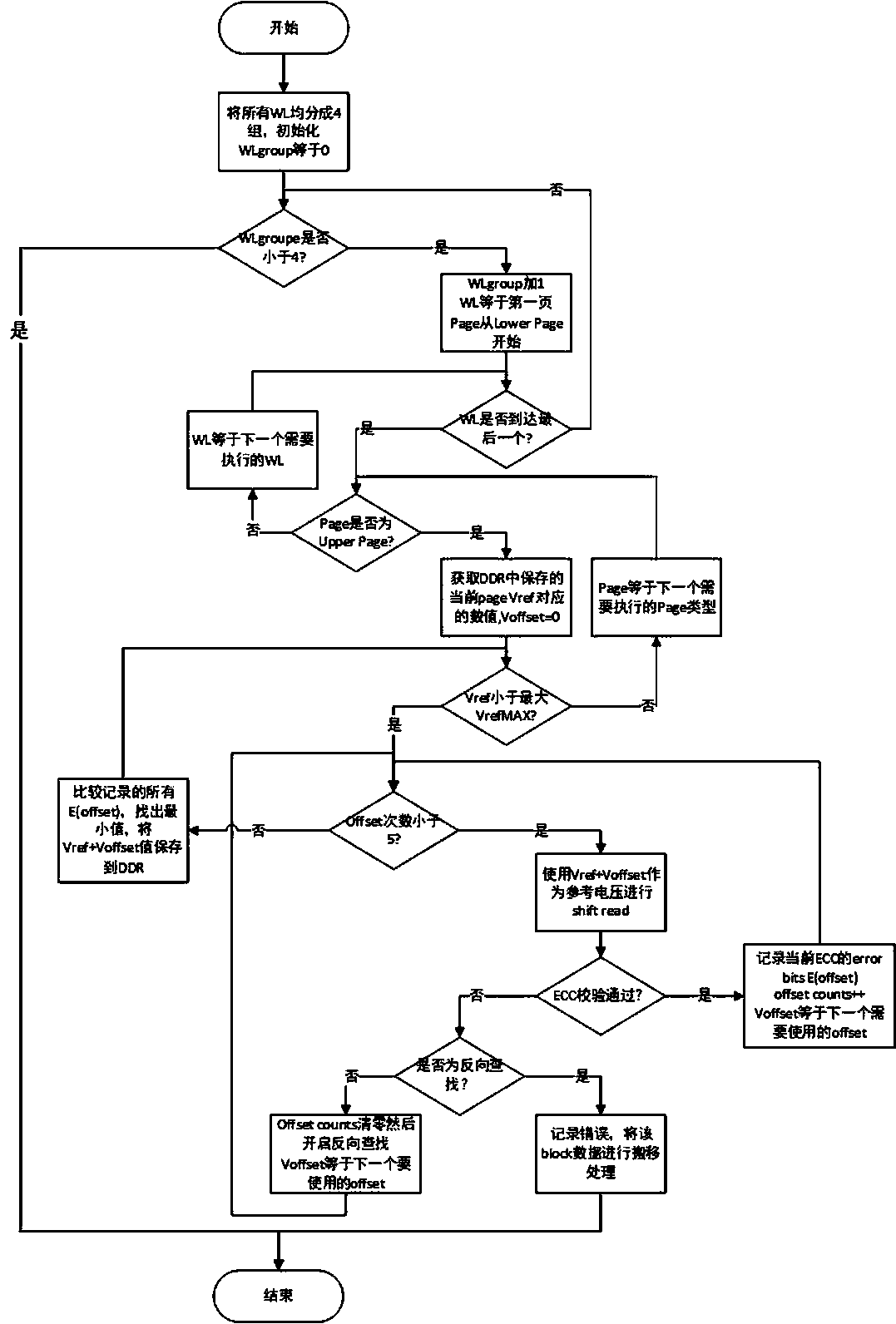
Method for calibrating NAND Flash read reference voltage on line in SSD
A technology of reference voltage and calibration voltage, which is applied in the field of memory, can solve problems such as data errors and achieve the effect of improving stability
- Summary
- Abstract
- Description
- Claims
- Application Information
AI Technical Summary
Problems solved by technology
Method used
Image
Examples
Embodiment 1
[0017] NAND Flash Read operation can be divided into normal read (normal read) and offset read (shift read). Normal read only needs to send the Read command; shift read needs to be set by the Set Feature command before sending the Read command. The reference voltage parameter read this time. The reference voltage parameter represents the read V currently used to read the page ref , different parameters correspond to different V ref . This method utilizes the characteristic that shift read can adjust the reference voltage, and obtains the best reference voltage when reading the current page by using a method of adjusting the reference voltage shift read multiple times, which is used for subsequent reading operations of the page and reduces data occurrence probability of error.
[0018] In this embodiment, a 2-3-2 coded 3D TLC including 256 Wordlines is taken as an example for illustration.
[0019] Since the characteristics of NAND Flash are expressed in units of blocks, al...
PUM
 Abstract
Description
Claims
Application Information
 - R&D Engineer
- R&D Manager
- IP Professional
- Industry Leading Data Capabilities
- Powerful AI technology
- Patent DNA Extraction
Browse by: Latest US Patents, China's latest patents, Technical Efficacy Thesaurus, Application Domain, Technology Topic, Popular Technical Reports.
© 2024 PatSnap. All rights reserved.Legal|Privacy policy|Modern Slavery Act Transparency Statement|Sitemap|About US| Contact US: help@patsnap.com


