I2C and USB compatible design circuit

A technology for designing circuits and circuits, applied in electrical digital data processing, instruments, etc., can solve problems such as I2C signal interface pin hardware design conflicts, communication mode selection conflicts, etc., to achieve flexible selection, resolve pin conflicts, and meet flexible applications Effect

Pending Publication Date: 2019-12-10
杭州凡诺电子有限公司
View PDF0 Cites 0 Cited by
  • Summary
  • Abstract
  • Description
  • Claims
  • Application Information

AI Technical Summary

Problems solved by technology

[0003] The object of the present invention is to provide a kind of I2C and USB compatible design circuit, to solve the hardware design conflict of USB signal interface and I2C signal interface pin of Atmel capacitive touch chip in the prior art, the selection conflict of communication mode question

Method used


Image

  • I2C and USB compatible design circuit

Examples


Embodiment Construction

[0015] The following will clearly and completely describe the technical solutions in the embodiments of the present invention with reference to the accompanying drawings in the embodiments of the present invention. Obviously, the described embodiments are only some, not all, embodiments of the present invention. Based on the embodiments of the present invention, all other embodiments obtained by persons of ordinary skill in the art without making creative efforts belong to the protection scope of the present invention.

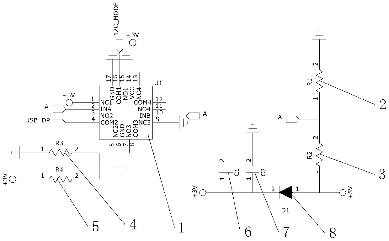
[0016] see figure 1 , the present invention provides a technical solution: an I2C and USB compatible design circuit, characterized in that it includes a compatible processing chip and a peripheral matching circuit connected with the compatible processing chip, and the peripheral matching circuit includes a resistor 1 and a resistor 2 , Resistor 3, Resistor 4, Capacitor 1, Capacitor 2 and diode, one end of resistor 1 is connected to +5V power supply, the other ...


PUM


Abstract

The invention relates to the technical field of capacitive touch chip circuits, in particular to an I2C and USB compatible design circuit. The device comprises a compatible processing chip and a peripheral matching circuit connected with the compatible processing chip, the peripheral matching circuit comprises a resistor I, a resistor II, a resistor III, a resistor IV, a capacitor I, a capacitor II and a diode; one end of the resistor I is connected with a + 5V power supply, and the other end is grounded after being connected with a resistor II in series; the anode end of the diode is connected with one end of the resistor I away from the resistor II; one end of the first capacitor and one end of the second capacitor are respectively connected with the negative electrode end of the diode,the other end of the first capacitor and the other end of the second capacitor are both connected with the ground, one end of the fourth resistor is connected with the + 3V power supply, and the otherend of the fourth resistor is connected with the third resistor in series and then connected with the ground.

Description

technical field [0001] The invention relates to the technical field of capacitive touch chip circuits, and the specific field is an I2C and USB compatible design circuit. Background technique [0002] Atmel capacitive touch chip (hereinafter referred to as TIC) supports USB signal interface and I2C signal interface respectively. However, the two interfaces cannot be compatible and designed on the same product, because the TIC pins conflict in hardware design; this defect cannot satisfy customers' flexibility in using the product. Contents of the invention [0003] The purpose of the present invention is to provide a kind of I2C and USB compatible design circuit, to solve the hardware design conflict of USB signal interface and I2C signal interface pin of Atmel capacitive touch chip in the prior art, the selection conflict of communication mode question. [0004] In order to achieve the above object, the present invention provides the following technical solutions: an I2C...

Claims


Application Information

Patent Timeline
Patent Type & Authority Applications(China)
IPC IPC(8): G06F13/42G06F13/38
CPCG06F13/382G06F13/4282
Inventor 郑亚利
Owner 杭州凡诺电子有限公司
Why Eureka
Try Eureka